Metal in the Board: Meeting the Challenge of Digital Power
This article is part of the TechXchange: Cool Designs.
New families of power semiconductors require new approaches in board design for thermal and power management. A number of board level solutions have emerged, divided into 12 major types segregated by:
- Thermal management technology- heat pipes, inlays, dissipation planes, etc.
- Current management- copper planes, embedded bus bars, discrete wiring or strips
- Board layup- number of layers, use of internal/external dissipator planes
The basic building blocks for “Metal in the Board” or “MiB” consist of:
- Metal based laminate
- Thick copper layers
- Thermal vias
- Thermal risers
- Metal inlays
- Encapsulated bus bars
- Bonded and/or embedded wires and strips
These building blocks offer a wide range of thermal management capabilities, and have been characterized in terms of the power densities they are capable of managing with less than 10 °C temperature rise through the board thermal path. Solutions typically range from 0.25 W/cm2 up through 35 W/cm2- through the board. This range of capabilities is proving to be critical as power conversion, management, and control becomes digital and advances in power semiconductor technology combined with the cost advantages of automated assembly drive development of new and smaller surface mount packaging.
High Power
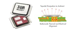
One of these is the “isometric” family of packages, developed by International Rectifier and marketed as the “DirectFET®.” A similar package is offered under license to IR by Infineon- the “CanPAK™”. These devices are “isometric” because they provide a balanced thermal pathway both into the board and, if necessary, out through the top of the package. This represents a significant advantage over other SMT power semiconductor packages such as the TO-252 “D2PAK” or TO-263 types, which require “gullwing” heat sinks if the board design is not capable of supplying a sufficiently low thermal resistance pathway (Fig. 1).
While the isometric types offer greater flexibility in management of the thermal path, they are also capable of currents well in excess of the 10 – 15 A typically considered the top end for conventional printed circuit boards. The power applications typically serviced by MOSFETs or IGBTs in isometric packaging involve currents from 50 to several hundred amperes, and managing these current levels involves a different and unique set of board design criteria.
Ampacity
Current flow through a conductor causes resistive power losses (I2R) in the form of heat, and at high current lev els the temperature increase becomes a factor in determining ampacity because the resistivity of the conductor changes with temperature. The relationship is linear, i.e., resistivity increases proportional to the change in temperature at a rate determined by the temperature coefficient of the conductor:
RT = RT0 × [(1 + a (T - T0)] (1)
Where:
T = Temperature at which resistivity is measured
T0 = Reference temperature (ambient)
a= Linear temperature coefficient (copper = 0.004)
RT = Resistivity at measurement temperature
RT0 = Resistivity at reference temperature
For a copper conductor, every 25°C increase in temperature means a drop of about 5% in maximum ampacity due to an increase in conductor resistivity, RT. Since this presents the probability of further power dissipation and temperature rise, MiB design practice must consider effective methods not only to control and reduce conductor resistivity, but also to provide low thermal resistance pathways for heat dissipation.
In a printed circuit board, ampacity depends on a number of different factors:
- Conductive + convective capability provided by spreading layers, ground layers, stack-up
- Ratio of track width to thickness
- Ambient temperature
- Adjacent high current tracks
- AC or DC current
- Presence and frequency of partial cross-section shrinkage
- Presence, number, and conductive cross-section of plated through holes in series with the conductor.
Therefore effective design needs to consider more variables than are normally addressed by the IPC-2152 current vs. temperature charts.
MiB
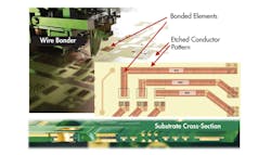
“Metal in the Board” or “MiB” includes a number of approaches where MiB building blocks are combined to provide effective high-current solutions. The “DWPCB” (discrete wire PCB) type is one of the most versatile. One of the commercially available versions of DWPCB is HSMtec, developed by the Austrian PCB manufacturer Häusermann GmbH. HSMtec uses 0.5 mm diameter copper wire and rectangular sectioned 0.5 mm thick copper strips (“profiles”) to provide discrete low resistance electrical and thermal pathways in the board as shown in Fig. 2.
There are a number of advantages to this solution compared to conventional thick copper or metal core boards:
- Conventional PCB processes ensure consistently high reliability
- Enhanced thermal and current pathways only where needed
- Cost of MiB limited to those nets needing MiB
- Wiring densities up to and including HDI enable logic and power integration
- FR-4 materials reduce CTE mismatch common to aluminum based substrates
- Board may be folded during assembly, providing photometric solutions for LED luminaires and eliminating daughter boards/connectors
The profiles and wires that make up the MiB components in a DWPCB board are bonded to tracks etched on inner layer cores, basically forming a sandwich consisting of the etched track and the bonded elements. This patented process ensures the uniform contact between the track and the wire/profile, which is essential for homogenous heat spreading and uniform conductor cross-sectional area. It also simplifies the layout task and/or conversion from conventional designs, as placement of the high current MiB components: the wires and profiles—will be done on what are essentially enlarged tracks on an inner or outer layer.
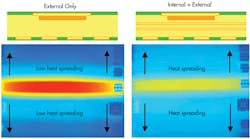
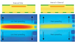
This arrangement provides a great deal of flexibility in stack-up configuration. Profiles/wires are bonded to a routing track, and thermal dissipation planes can be located on the same layer or on a facing layer co-axial with the MiB track. Facing layer thermal planes have been seen to improve thermal performance as shown in Fig. 3.
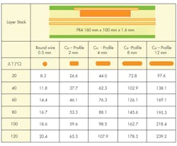
Design guidelines include ampacity tables based on actual thermographic observations of different layup configurations. As shown in Fig. 4, the DWPCB type is suited for “medium” power applications with nominal currents up to about 140 A (40 °C temp rise).
In combination with thermal vias or inlays this value can run to over 300 A depending on duty cycle. Other MiB types covered in BPA’s report are designed for high current applications (250 - 1000 A) — typical of Hybrid/Electric Vehicle and high power rectification.
The medium current capability, heat-spreading characteristics, and design versatility of the DWPCB type make it a cost-effective alternative to logic boards, busbars, and cable in an expanding range of applications.
Electromobility Powertrain
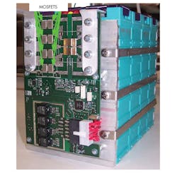
The Lithium-ion battery pack shown in Fig. 5 provides a mean value of 100 A with peaks to 300 A for a light electric vehicle.
Both weight and size are critical in this application as any increase in mass directly affects vehicle range. To save both, a battery management system consisting of control logic and eight DirectFET™ power devices is mounted right on the front of the battery pack. A DWPCB solution proved ideal for integrating the control logic with the power section, reducing two pcbs to one and eliminating the associated connectors and cabling.
The design challenge involved routing 100 / 300 A through an FR-4 circuit board to the DirectFETs and out to the load. Häusermann’s versatile DWPCB technology enabled several different options to be considered, ranging from single-layer power distribution to a multi-level design with integrated thermal vias and dissipation planes.
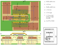
The most cost-effective design is shown in Fig. 6.
In this layout, the profiles have been bonded to an inner core consisting of High Tg FR-4 clad with 2 oz. (70µ) copper. Since the profiles are all on the same reference plane, setup and run time for the bonding equipment is optimized and the subsequent mass-lamination process has a less complex embedding task compared to a design where the profiles are on several different layers. The embedded profiles also free up real estate on the surface of the board: the area needed for the high-current tracks is confined to the via arrays used to access the embedded profiles,while the wide tracking necessary to support the profiles is confined to the internal layer.
Microvias
The high current profiles are accessed by arrays of laser microvias. This technique is growing in popularity in a number of MiB types, because although laser vias are typically 100 µ in diameter or less, what counts in an MiB application is the length of the conductive element (in this case, depth of the via) and cross-sectional area of copper available as a thermal pathway.
The copper area can be determined by the difference in surface area between the two circles formed by the via drilled diameter and inside plated diameter. The thermal resistance of the via array is therefore determined by:
RѲarray = l / k × (Nvias × {π × [(D1/2)2 - (D2/2)2]}) (2)
Where:
l = Depth of via
k = Conductivity of copper (approx. 380 W/m-K)
D1 = Drilled diameter
D2 = Finished (plated) hole diameter
Nvias = Number of vias in the array
And, since laser microvias are very small and are drilled at effective hit rates well in excess of 10,000 per minute (for CO2 “copper direct” process), a lot of them can be placed in a thermal pad. An array of 1296 microvias in a 100 mm2 thermal pad will present a thermal resistance of about 0.01 W/°C: about the same as the solder joint used to bond the device’s thermal slug to the pad!
In addition to the microvias used to access the buried profiles, the design increases the dissipation area available to the device by running thermal vias down to bottomside dissipation planes. Here, the fabrication challenge entails drilling bulk copper, which involves chiploads less than one-third those of FR-4. However, thermal vias are basically heat pipes, so any nailheading that occurs at the layer 3 joint in this design will not compromise electrical performance. The objective is to get a clean hole and homogeneous copper deposit for thermal transfer. Thermal via arrays can be very effective ways to get heat down through the board to a backside dissipation plane: the conductivity of a typical array is between 20 – 30 W/m-K which is over 100X that of FR-4.
Managing the power tracks inside the board leaves room for signal and control wiring on the outer layer, and the gate signals for the parallel FETs are run on the surface of the board. Typical dimensions for a layout of this kind are shown in Fig. 6 as well as the positioning of the profiles on the etched core carrier tracks. Gaps between the profiles have been expanded for clarity: the gap volume represents a variation of less than 0.1% of the total conductor volume. The result of this design is the clean footprint shown in Fig. 7.
MiB Cost
Faced with a solution presenting this level of innovation and simplicity, the first question is almost certainly “but how much does it cost?” While the applications requiring this solution are driven primarily by reliability and performance (electromobility lifetimes range from 15 to 25 years, and improvements in functional density mean decreases in weight and volume with corresponding increases in operational autonomy), the cost equation is zero sum, i.e., an alternative technology either has to come in at parity and be ready to follow the same cost reduction trajectory as the assembly it replaces, or offer an order of magnitude improvement: in cost, performance, reliability, or a combination of all three.
The design example presented above essentially accomplished two objectives:
- it enabled the use of the latest generation of isometric power packages, in the process reducing board real estate necessary for thermal and current management by some 30%
- it enabled a reduction in volume and weight through a combination of reduced power board area, elimination of the controller daughterboard, replacement of the vertical plate heat sinks required by PIH (pin-in-hole) TO devices with smaller finned assemblies and chassis standoffs, and replacement of high current cabling with direct connections to the power bus.
Considering only the reduction in parts count and assembly costs, the MiB solution provided a savings of about 13% compared to the initial design. But the potential savings could be greater when taking into account the additional benefits of weight and volume reduction. The cost savings obtained from reduced weight and volume is the subject of ongoing analysis.
The result of this design has been a printed circuit solution to the challenges of heat dissipation and power distribution typical of medium power applications using the latest SMT packages. The surface mount nature of these devices means the board must be capable of providing low resistance thermal as well as electrical pathways. This design exemplifies how conventional printed circuit technologies, including laser and mechanically drilled holes , may be combined in innovative buildups to meet the challenges of Digital Power.
*NOTE*
Information for the Metal In The Board article was derived from a February 2013 BPA Consulting report on “Metal In the Board- Opportunities for Printed Circuit Boards Providing Enhanced Thermal and Power Management.” In the report, BPA (www.bpaconsulting.com) take the first comprehensive look at what Digital Power means for printed circuits. In over 250 pages including 360 illustrations, charts, and tables, the report presents the fundamentals of thermal and power management for PCBs, identifying and profiling a number of emerging board level solutions and applications. The report includes both technology and business analysis as well as international market forecasts by technology, application, and region.
