Heterogeneous 2.5/3D Chip Design Requires Integrated Tools
What you’ll learn:
- Why co-optimization is needed when designing 2.5D and 3D chips.
- The tools provided by Siemens for 2.5D and 3D chip design and packaging.
The latest high-performance chips often employ 2.5D and 3D chip technologies like chiplets to deliver their functionality within the required cost, power, and performance requirements. Companies are moving from system-based optimization to design-based optimization as system design and packaging become more complex.
I talked with Kevin Rinebold, Account Technology Manager for Advanced Packaging at Siemens EDA, about the changes in the industry, Siemens’ tools that address this space, and the company’s “cockpit.”
The workflow for 2.5/3D chip design requires quite a bit of planning and simulation to verify that a chip can be produced and meet the design requirements (Fig. 1). The process can be streamlined by using structured design frameworks such as assembly design kits (ADKs), package design kits (PDKs) and chip design kits (CDKs) that help design teams take advantage of specific chip fabrication technologies.

A more detailed flow diagram (Fig. 2) highlights the need for co-optimization between design, implementation, and verification. All of this is needed to make sure final chip production will be successful and the chips will meet their design requirements.

Siemens offers an integrated solution (Fig. 3) built around a single tool and system hierarchy to go from planning to prototyping and manufacturing. Among the tools in the mix are Xpedition design software, Calibre design verification, and SimCenter simulation and test platform. This includes chip and chiplet design at the RTL level through chip packaging. These tools can be used individually and with third-party tools.

The Siemens Xpedition Substrate Integrator is one of the tools available from Siemens; it addresses everything from mechanical design to chiplet and interposer design (Fig. 4). Product lifecycle management (PLM) and design for test (DFT) are part of the package, as is co-simulation support for thermal and mechanical aspects of the design.
 handles planning, prototyping, and system co-optimization.")
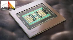
Check out more videos and articles in Chiplet Summit 2024 and the TechXchange: Chiplets - Electronic Design Automation Insights.