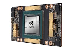
The big news at this year’s virtual GPU Technology Conference (GTC) was Nvidia’s release of the A100 (Fig. 1). The A100 with its 54.2 billion transistors can get a bit toasty with a max thermal design power (TDP) of 400 W, and a large array of modules can be connected using the built-in NVLinks. Each module supports 600 GB/s of NVLink bandwidth in addition to the 64 GB/s PCI Express (PCIe) Gen 4 interfaces. The PCIe interfaces support SR-IOV.
The A100 is based on the company’s new Ampere architecture that provides a significant performance boost compared to the earlier V100 Volta and Turing architectures. Included is 40 GB of HBM2 on-module memory for the A100 with a memory bandwidth of 1555 GB/s. There’s also a 40-MB L2 cache that’s almost seven times that of the V100.
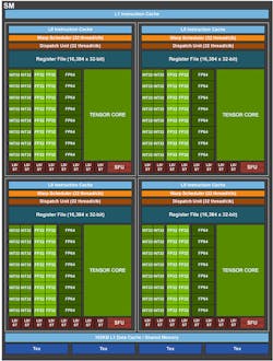
Seven GPU processing clusters (GPCs) and seven texture processing clusters (TPCs) are incorporated into the A100, along with 16 streaming multiprocessors (SMs) per GPC (Fig. 2). The ten 512-bit memory controllers support five HBM2 memory stacks. The SMs support all data types. A new shared-memory-based barrier unit provides asynchronous barriers to handle new copy instructions. The systems support 32 threads/warp and 64 warps/SM.
Usually, multiple A100s are tied to the NVLink interface, enabling very large models to be run across an array of chips. A new feature is Multi-Instance GPU (MIG), which allows the opposite to occur by splitting up the GPU resources into dedicated and protected islands of computation. Up to seven instances can be defined running CUDA applications. CUDA 11 is Nvidia’s latest programming environment.
Each MIG instance has separate and isolated paths through the entire memory system. Other resources like the on-chip crossbar ports, L2 cache banks, memory controllers, and DRAM address buses are also allocated to these logical islands. This provides predictable throughput and latency. L2 cache allocation and DRAM utilization will not be affected by the operation of other instances. Error and fault isolation are maintained within each instance.
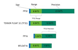
The A100 supports a range of numeric formats, including Tensor Float 32 (Fig. 3). It provides the range of FP32 but trims the number of significant bits, thereby allowing A100 designers to implement matrix calculations more efficiently. The system also supports FP16 and BFLOAT16 along with a host of integer formats. All of these are available and optimized for machine-learning (ML) model acceleration.
Peak performance for 64-bit floating point is 9.7 teraFLOPs (TFLOPS). At the other end of the spectrum is the INT4 performance of 1248 TOPS. These numbers are impressive, but Nvidia’s platform also implements sparsity optimization.
ML and artificial-intelligence (AI) applications are a prime target for the A100. The neural-network models for ML/AI applications typically utilize sparse matrix operations. The sparsity support allows these operations to be performed more quickly. For the Tensor Float 32, the standard 156 TFLOPS doubles to 312 TFLOPS with sparsity support. FP16 and BFLOAT16 also benefit in a similar fashion, in addition to the integer support.
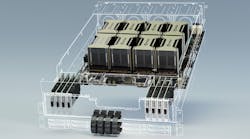
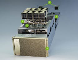
The A100 is being used in a number of form factors, such as the DGX A100 (Fig. 4). The box delivers 5 petaFLOPS of performance in a single box. The DGX A100 consists of eight A100 modules, six NVSwitches with 4.8 TB/s of bandwidth, nine Mellanox ConnectX-6 200-Gb/s interface cards, dual 64-core AMD CPUs, and 15 TB of Gen 3, NVMe SSDs with a peak bandwidth of 250 GB/s. It’s based on the HGX A100 motherboard.
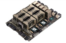
The HGX A100 motherboard hosts eight A100 modules connected by a new, faster NVSwitch matrix (Fig. 5). The platform also has PCI Express switches that support 200-Gb Ethernet NICs like the Mellanox ConnectX-6 as well as NVMe storage. A pair of high-performance CPUs can be connected to the PCIe switches. A four-A100 version is also available. Both support GPUDirect Storage, which lets the GPUs work with the NVMe storage, bypassing the CPU.
Nvidia continues to deliver more performance by orders or magnitude every couple of years. That alone would be impressive, but it’s really the software infrastructure that the company has built around its hardware that makes it work. This starts with CUDA and includes everything from the Isaac SDK for robotics, to cuDNN, to its TensorFlow support. Even the new MIG support is integrated with its Kubernetes container management system.
