>> Electronic Design Resources
.. >> Library: Article Series
.. .. >> Series: The Graphics Chip Chronicles
.. .. .. >> Introduction to this Series
.. .. .. << HP's Artist Graphics Chip
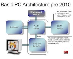
Integrated graphics have been with us since 1991 in the workstation space, and since 1995 in the PC. They have now found their way into smartphones, tablets, cars, game consoles, and many other devices.
Integrated graphics have evolved from being part of the chipset to being integrated within the CPU. Intel did that first in 2010. AMD followed them with the Llano in 2011, but with a much bigger and more powerful GPU. In between, we saw clever and innovative designs from various suppliers, many of them no longer with us.
May 1995—One of the first examples of integrating a graphics controller with other components was the SPARC enhancement chipset from Weitek. This chipset consisted of two parts: the W8701 SPARC microprocessor and the W8720 Integrated Graphics Controller (IGC). The W8701 integrated a floating-point processor (FPP) into a SPARC RISC microprocessor. It ran at 40 MHz and was socket- and binary-compatible with the SPARC integer unit (IU) standard.
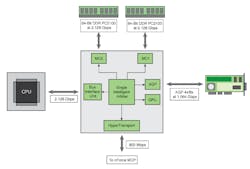
June 1995—Taiwan-based Silicon Integrated Systems introduced the SiS6204, the first PC-based integrated graphics controller (IGC) chipset for Intel processors. It combined the northbridge functions with a graphics controller and set the stage for a new category—the IGC.
SiS developed two IGCs, the 6204 for the 16-bit ISA bus, and the 6205 for the newer PCI bus. The graphics controller offered an integrated VGA with resolution up to 1280 ×1024 × 16.8 million colors (but interlaced), a 64-bit BitBLT engine with an integrated Philips SAA 7110 Video Decoder Interface that provided YUV 4:2:2 support, color-key video overlay support, color space converter, integer video scaling in 1/64th unit increments and VESA DDC1 and DDC2B signaling support . It offered UMA capability with SiS’s 551x UMA chipsets. Most importantly, it proved what one could integrate into a small, low-cost chip. SiS and ALi were the only two companies initially awarded licenses to produce third party chipsets for the Pentium 4.
January 1999—In the late 1990s, workstation giant Silicon Graphics Inc (SGI), was trying to meet the threat of the popular and ever-improving x86 processors from Intel. SGI developed the Visual Workstation 320 and 540 workstations using an Intel Pentium processor and designed the Cobalt IGC. It was a massive chip for the time with over 1,000-pins, and it cost more than the standard CPU. It also highlighted the potential performance boost of a unified memory architecture (UMA), one where the graphics processor shared the system memory with the CPU. It made up to 80% of the system RAM available for graphics. However, the allocation was static and only adjusted via a profile.
April 1999—Intel had been leading the industry with consolidating more functions in the CPU. In 1989, when it introduced the venerable 486, it incorporated an FPP, the first chip to do so. A decade later, the company introduced the 82810 IGC (codenamed, Whitney).
September 1999—David Orton, who led the development of the Cobalt chipset while VP of Silicon Graphics’ advanced-graphics division, left SGI and became President of ArtX. The company revealed its first integrated graphics chipset with a built-in geometry engine at COMDEX in the fall of 1999, then marketed by Acer Labs of Taiwan. Seeing that, Nintendo contacted ArtX to create the graphics processor (called the Flipper chip) for fourth game console, the GameCube. Then in February 2000, ATI announced it would buy ArtX.
June 2001—SiS introduced transfer and lighting (T&L) to its IGC. Transformation means producing a two-dimensional view of a three-dimensional scene. Clipping means only drawing the parts of the scene that are in the image after the rendering has completed. Lighting is the process of altering the color of the various surfaces of the scene based on lighting information. Arcade game system boards used hardware T&L since 1993, and it was also used in home video game consoles since the Nintendo 64’s Reality Coprocessor GPU (designed and developed by SGI) in 1996. Personal computers implemented T&L in software until 1999.
With the introduction of geometry processing and T&L, the IGC evolved into the IGP — integrated graphics processor.
June 2001—Nvidia introduced its IGP the nForce 220 for AMD Athlon CPU.
The nForce was a motherboard chipset created by Nvidia for AMD Athlon and Duron (later it included support in the 5-series up for Intel processors). The chipset shipped in three varieties; 220, 415, and 420. 220 and 420 were very similar, with each having the integrated GPU.
When Intel moved from a parallel bus architecture to a serial link interface (copying the hyperlink design from AMD), they also declared Nvidia’s bus license invalid. After a protracted legal battle, Nvidia won a settlement from Intel, and in 2012 exited the IGP market, leaving only AMD, Intel, and small Taiwanese supplier Via Technologies. Every other company in the market was either bought or driven out of the market by competition.
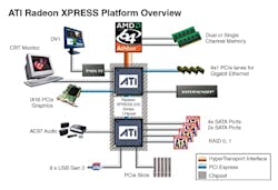
January 2002—Two years after its acquisition of ArtX, ATI introduced its first IGC, the IGP 320 (code named ATI A3) IGC.
Four years after ATI introduced the IGC, AMD bought ATI to develop a processor with a real integrated GPU. At the time, Dave Orten was ATI’s CEO. However, it proved harder to do than either company thought. Different fabs, different design tools, and clashing corporate cultures made it an incredibly difficult task.
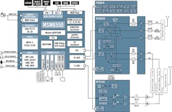
July 2004—Qualcomm introduced its first integrated graphics processor in the MSM6150 and MSM6550 using ATI’s graphics Imageon processor.
The graphics processor could support 100,000 triangles per second and 7 million pixels per second for console-quality gaming and graphics.
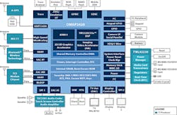
October 2005—Texas Instruments introduced the OMAP 2420 and Nokia introduced in the N92 and then the N95.
TI used an Imagination Technologies’ PowerVR GPU design for their OMAP processors. The company was successful with the OMAP in mobile phones until about 2012 when Apple and Qualcomm-based phones took the market by storm.
June and November 2007— Apple introduced the iPhone in the United States in June, and Qualcomm introduced the Snapdragon S1 MSM7227 SoC in November of the same year. Every chip company at that point had developed SoCs with integrated GPUs, primarily for the smartphone market. Apple used Imagination Technologies’ GPU design, and Qualcomm used ATI’s mobile GPU Imageon technology. In January 2009, AMD sold its Imageon handheld device graphics division to Qualcomm.
2008—Nvidia introduced the Tegra APX 250 SoC with a 300-to-400 MHz integrated GPU and a 600 MHz ARM 11 processor. Audi incorporated the chip in the entertainment system of its cars, and other car companies followed. In March 2017, Nintendo announced it would use a later generation of the Tegra in its Switch game console.
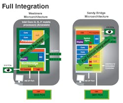
January 2010—In the PC market, Intel beat out AMD and introduced its Clarkdale and Arrandale processors with Ironlake graphics. Intel branded them as Celeron, Pentium, or Core with HD Graphics. The GPU’s specification was 12 execution units (shaders), delivering up to 43.2 GFLOPS running at 900 MHz. The IGP could also decode an H264 1080p video at up to 40 fps.
Intel built the first implementation, Westmere, as a multi-chip product in a single case. The CPU using Intel’s 32-nm process and the GPU based on 45-nm.
The most significant difference between Clarkdale and Arrandale is that the latter had integrated graphics. Intel manufactured the fully integrated 131mm2 processor, Sandy Bridge, as a 4-core 2.27 GHz processor with the integrated GPU in its 32-nm fab.
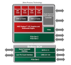
January 2011—When AMD bought ATI, Hector Ruiz was president of AMD and Dave Orton was president of ATI. Orton left AMD in 2007, and Ruiz left in 2008, the architects of the acquisition and the dream of building a CPU with integrated graphics at AMD. It took three years and several new CEOs after Ruiz left before AMD could introduce an integrated GPU-CPU, which they named an APU—for “accelerated processor unit.” The first product, in 2011, was the Llano, and the internal code name for the processor was Fusion.
The Llano combined the four-core K10 x86 CPU and Radeon HD 6000-series GPU on the same 228mm2 die. AMD had it fabricated at Global Foundries with the 32-nm process.
November 2013—Sony introduced PlayStation 4 game console, and Microsoft launched the Xbox One, both based on a custom version of AMD’s Jaguar APU. Sony's APU used an eight-core AMD x86-64 Jaguar 1.6 GHz CPU (2.13 GHz on PS4 Pro) with an 800 MHz (911 MHz on PS4 Pro) GCN Radeon GPU. Microsoft used an eight-core 1.75 GHz APU (2 quad-core Jaguar modules), and the Xbox One X model contained a 2.3 GHz AMD eight-core APU. The Xbox One GPU ran at 853 MHz, the Xbox One S at 914 MHz, and the Xbox One X at 1.172 GHz using AMD’s Radeon GCN architecture.
Today—The integrated GPU or iGPU is more popular than anything else on the market. It is cost-effective and powerful enough for most graphics chores. It is also seeing acceptance in power-demanding workstation applications.
The iGPU is the dominant GPU used in PCs, and it is in 100% of all game consoles, 100% of all tablets and smartphones, and around 60% of all automobiles, which translates to about 2.1 billion units.
GPUs are incredibly complicated and complex devices with hundreds of 32-bit floating-point processors called shaders and crammed with millions to billions of transistors. That could only have been accomplished due to the miracle of Moore’s Law. Every day you engage with multiple GPUs, in your phone, PC, TV, car, watch, your game console, and through the cloud. The world would not have progressed to where it is without the venerable, ubiquitous GPU.
>> Electronic Design Resources
.. >> Library: Article Series
.. .. >> Series: The Graphics Chip Chronicles
.. .. .. >> Introduction to this Series
.. .. .. << HP's Artist Graphics Chip

