New Low-Cost FPGA Comes in Compact InFO Package
What you’ll learn:
- How InFO packaging uses 60% less area and is 70% thinner.
- How UltraScale+ FPGAs take advantage of InFO.
TSMC supports the ultra-compact InFO (Integrated Fan Out) packaging technology and Xilinx is taking advantage of it with its new 16-nm UltraScale+ family of FPGAs. Chips will be available in the InFO form factor as well as conventional flip-chip packages. Members of the family donning these smaller packages include the Artix UltraScale+ and the Zynq UltraScale+ SoC with dual- and quad-core Arm Cortex-A53 processors.
The InFO package, measuring 11.5 × 9.5 mm, uses 60% less area than a flip-chip package and is 70% thinner (Fig. 1). Xilinx also reduced the thermal and power requirements for these cost-optimized chips.
The Artix UltraScale+ supports 16-Gb/s transceivers. Also incorporated is hard logic for PCI Express (PCIe). Certification for PCIe Gen 4 support for the AU10P and AU15P is in the works. The smaller AU10P comes with 96K logic cells, 44K lookup tables (LUTs), and 3.5 Mb of RAM. Xilinx chose to keep the DSP ratio high with 400 DSP slices in the AU10P and 576 for the AU15P. Both have a dozen gigabit transceivers. Furthermore, the chips feature up to 192 Gb of aggregate bandwidth.
The Artix UltraScale+ targets applications like advanced sensor systems, high-speed networking, and ultra-compact “4K-ready” video broadcasting. The chips feature multi-level security, too, including resistance to differential-power-analysis (DPA) side-channel attacks. These security features, found across the UltraScale+ platform, also include RSA-4096 authentication, AES-CGM decryption, and Xilinx’s proprietary Security Monitor IP. The monitor adapts to security threats throughout the product lifecycle.
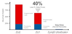
Zynq UltraScale+ ZU1 extends the low end of the SoC family. Developers can scale using higher-end SoCs like the ZU2 and ZU3. The ZU1 is available in dual and quad versions of the Arm Cortex-A53 processors. The ZU1 has been designed to use 40% less power than the ZU2, but the FPGA fabric size is only 20% less than the ZU2. It’s possible to power down unused blocks for deep sleep, consuming under 200 nW of power (Fig. 2).


