Arm Pushes Performance Limits With V1 Server CPU Core
Arm is trying to move within striking distance of Intel and AMD's performance lead in the data center market with a new high-performance bracket in its Neoverse family of server CPU cores.
Arm said the Neoverse V1 core is its highest performance CPU core and that it would serve as a blueprint for central processing chips that are faster than Intel's Xeon Scalable and AMD's EPYC server chips. Based on its Zeus microarchitecture, the 64-bit V1 core is focused on AI and high-performance computing (HPC) workloads in massive cloud data centers and supercomputers.
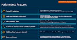
Arm upgraded the V1 core's microarchitecture with wider and deeper processing pipelines and added SVE technology to give the CPU what it claims is industry-leading per-core performance.
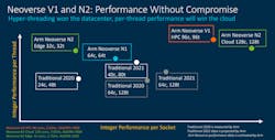
The V1 core has 50% more single-threaded performance than its predecessor, the Neoverse N1 core, due to microarchitecture improvements. The V1 pumps out 10% more performance than the N2 core that is a more direct successor to the N1, targeted at cloud servers and other data infrastructure. Arm said the V1 could be slapped on server chips based on the 7- or 5-nm nodes.
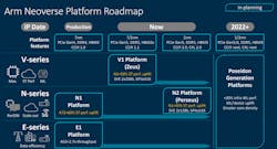
The company expanded its server CPU roadmap with the V1 and N2 cores last year.
The V1 is a large generational leap in performance over the N1 core introduced in 2018. Amazon uses the N1 core in its homegrown 64-core Graviton server CPU and Ampere Computing in its 128-core Altra Max CPU. Both chips are said to have significant gains over Intel’s “Cascade Lake” Xeon and AMD’s “Rome” EPYC chips in performance per watt at a more moderate cost.
“With the V1 core, you get Arm's best performance per thread,” said Chris Bergey, vice president and general manager of Arm's infrastructure business, in a briefing with reporters and industry analysts. “The V1 platform is a revolution in high-performance computing, and it delivers a massive performance uplift over the N1."
Arm said the 64-bit CPU core is ideal for server-grade processors with 32 to 128 single-threaded cores in power envelopes of 80 watts to 350 watts. But it signaled that the sweet spot is around 96 cores based on its V1 blueprints on the same silicon die. Arm said partners could configure caches, clock frequency, core counts, and other features of server chips based on the V1 core.
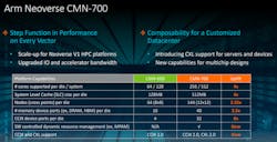
To that end, it also announced its most advanced mesh interconnect, CMN-700, which can be used to equip the V1 and N2 cores with DDR5 DRAM and HBM memory interfaces. It supports industry-standard protocols, including PCIe Gen 5, CCIX, and CXL, that are used to attach the CPU to GPUs, FPGAs, and other server accelerators—or install it in a system-in-package (SiP).
The power efficiency of Arm's CPU cores has transformed it into the gold standard in the global smartphone market. It is also gaining ground in personal computers with Apple's M1 processor. But the semiconductor industry's leading draftsman is also attempting to apply the principles of power efficiency and flexibility to data centers with its Neoverse family of CPU cores that came out in 2018 when it promised average performance gains of at least 30% per generation.
While it does not develop chips itself, Arm is trying to lure in technology giants, such as Amazon and Microsoft, to buy its blueprints and use them to build server-grade processors better suited for their demands than Intel's Xeon Scalable CPUs. Arm also licenses templates to startups, like Ampere Computing, trying to take the performance crown from AMD's EPYC server processors.
The company is striking at the heart of the high-end data center market with its N2 core, based on its "Perseus" microarchitecture, which has what it contends is industry-leading performance per watt. The N2 core is designed to deliver higher core counts and a "balanced" ratio of power to performance, and it can be deployed from data centers to 5G base stations and other areas.
But it is pulling out all the stops with the V1 core, pushing performance at all costs—even at the expense of power efficiency and area—to win more slots in supercomputers and data centers. Arm said that it started supplying the V1 core—part of its new V-series CPUs—to partners at the end of 2020, and they are on pace to start shipping server CPUs based on it by the end of 2021.
SiPearl is buying the blueprints to the V1 core to roll out a high-performance CPU with 72 cores on top of custom accelerators with four HBM2 lanes and up to six DDR5 interfaces for Europe’s exascale supercomputer. The CPU at the heart of the Rhea supercomputer will be based on the 6-nm technology node from TSMC and could start shipping by late 2021 or 2022.
The Center for Development of Advanced Computing (C-DAC) in India has announced it will join SiPearl and South Korea's ETRI in licensing the V1 for its national exascale supercomputer.
One of the HPC improvements in the V1 is its Scalable Vector Extensions, or SVE, technology, which wrings more performance and power efficiency out of AI, HPC, and other chores that take advantage of vectors. The more of these vectors the CPU can handle simultaneously—and the wider the vector pipelines in the CPU core itself—the more processing horsepower the CPU has.
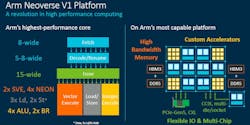
The V1 core integrates a pair of 256-bit wide vector processing pipelines that can handle SVE instructions. These internal processors can double as four 128-bit NEON engines, the previous generation of Arm's SIMD instruction set. SVE doubles the computational throughput of the 128-bit pipelines in the N1 core and can handle AI workloads using the popular bfloat16 data format.
The V1 is the Arm's first CPU core to leverage the SVE technology. Arm partnered with Fujitsu to develop the technology currently at the heart of Fugaku, the fastest supercomputer in the world.
While not on the same level as Nvidia's GPUs, Xilinx's FPGAs, or other accelerators in terms of parallel processing muscle, the V1 core can handle vector-heavy workloads, including machine learning, more efficiently than its predecessor. Arm said the V1 core improves vector processing more than 75% over its predecessor, the N1 core. That augments the ability of the CPU to run machine learning and other jobs instead of offloading them to GPUs or other accelerators.
Arm frequently adds special-purpose groups of instruction, or extensions, to its instruction set architecture (ISA) that can be enabled or disabled by its silicon partners and taken advantage of in software as needed. The 256-bit SVE accelerators in the V1 core correspond to the AVX-512 engines in Intel’s Xeon Scalable CPUs and the dual 256-bit FMA engines in AMD’s “Milan” CPUs. Arm said SVE is also engineered for ease of programming and software portability.
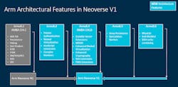
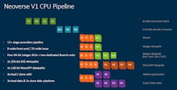
As opposed to the N2 core, which is based on the latest Armv9 architecture, the V1 brings the best of the Armv8-A architecture to upgrade performance, power efficiency, and scalability. The massively superscalar CPU sports a 15-wide instruction issue stage that feeds the 256-bit SVE pipelines and other functional blocks, including the branch units, load and store units, and ALUs. The V1 core fits all the performance features in the same 11-stage accordion pipeline as the N1.
"The design philosophy of the V1 was 'performance first,' so we widened the microarchitecture and made buffers and queues deeper to accommodate more instructions in flight," Bergey said.
Arm said the V1 cores are filled front-to-back with microarchitecture improvements. On the front end, the branch prediction unit is decoupled from the instruction fetch pipeline, which allows the CPU to run ahead and prefetch instructions into the L1 cache. The company enlarged the branch target buffers in the V1 to handle software with larger instruction footprints and reduce latency.
Arm said that means the V1 core should mispredict instructions less often and also stall less often while running AI and other workloads in supercomputers and power-hungry data centers.
The mid-core pipeline in the V1 incorporates a "micro-operation" cache that serves as the CPU's L0 instruction cache, fetching and dispatching eight instructions per cycle, which is double the throughput of Arm's N1. The improved cache keeps the V1 core loaded with instructions to run, which accelerates server and other data infrastructure workloads that frequently use smaller kernels.
Furthermore, it enlarged the out-of-order (OoO) execution pipeline in the V1 and accompanying load and store buffers, giving it the ability to handle more memory and core accesses in parallel. Arm said that it integrated another 64-bit ALU and another branch prediction unit in the V1 core, which, along with other mid-core improvements, results in gains of 25% in integer performance.
The V1 core also brings more bandwidth for load and store addresses and memory and I/O. The company said that it improved the memory management unit (MMU) in the V1 core, which also fills its L2 and L3 caches 15% faster than its predecessor. The company also improved the data prefetching technology in the V1, which adapts to the aggressiveness of different CPU designs.
Arm said the V1 core brings the same dispatch throttling (DT) and maximum power mitigation mechanism (MPMM) features as the N2 core to help keep it within thermal and power budgets. For scalability, the V1 core features memory partitioning and monitoring (MPAM) to prevent any single process running in the CPU core from hogging system cache—or other shared resources.
The microarchitecture improvements in the V1 core result in a 50% increase of instructions per clock at the same node and clock frequency as the N1. The trade-off is the V1 needs 70% more die area to accommodate the larger vector pipeline and other performance features. Arm said the V1 could also be manufactured on the 5-nm process node to negate some trade-offs.
Based on internal performance tests, Arm said that 96-core server processors based on the V1 cores provide major gains in performance over not only previous generations of Intel's Xeon Scalable CPUs and AMD's EPYC server processors but also 128-core server chips based on the N2.
“Our competitors are not standing still,” Bergey said. But the company said chips based on V1 would be able to compete Intel's latest "Ice Lake" Xeon or AMD's "Milan" EPYC chips rolling out in 2021.
Along with its CPU improvements, Arm also announced its latest mesh interconnect to arrange the V1 core on the processor die, serving as the connective tissue of future server chips based on Arm's CPU cores. The coherent mesh network interconnect, CMN-700, delivers a large boost in performance over the CMN-600, which was specifically designed to be used with the N1 core.
Arm said the interconnect gives its customers more flexibility to customize the CPU, surround it with on-die accelerators or other intellectual property (IP) parts in the final all-in-one silicon chip, or supplement it with memory, accelerators, or other paraphernalia to wring out performance at the level of the system. The industry demands flexibility; design freedom to achieve the right level of compute for the right application," Bergey said in a blog post detailing the V1 core.
The interconnect also supports the second-generation compute express link (CXL) to connect GPUs, FPGAs, or other accelerators to a server to offload AI or other chores taxing on the CPU.
Its customers can also use CMN-700 to integrate DDR5 memory interfaces and HBM2E for high bandwidth memory to the V1. The interconnect has industry-standard protocols, including PCIe Gen 5 to attach accelerators to the CPU within the server. The cache coherent interconnect for accelerators (CCIX) standard can be used as the primary CPU-to-CPU interconnect in a socket.
The CCIX technology doubles as a die-to-die interconnect for chips wrapped in advanced packaging or based on chiplets. “We give our partners the flexibility to incorporate on-die, specialized accelerators," Bergey said. "They also have the freedom to right-size the I/O and leverage chiplet and multi-chip capabilities to push core count and performance but by combining smaller dies that offer better yields and costs."
"We think this is the direction HPC is headed," he added.
