What’s the Difference Between HBM3 and HBM2E: A New Frontrunner
What you’ll learn:
- The differences between HBM3 and its predecessor, HBM2E.
- Why the HBM3 standard upgrade is significant.
Use of artificial intelligence and machine learning (AI/ML) is expanding rapidly with no end in sight, and enterprise applications’ reliance on it will only grow over time. From 2012 to present day, AI training capabilities have skyrocketed by a factor of over 300,000, causing memory bandwidth and capacity to become more of a performance bottleneck. As data centers continue to push their high-performance-computing (HPC) and AI/ML applications even further, they’re looking for a much-needed increase in bandwidth, alongside better efficiency.
This is where more tailored memory technologies such as high bandwidth memory (HBM) come into play. It’s no secret we’re starting to see more of HBM3 now that JEDEC officially announced the standard for it in January, setting the stage for improved performance in AI/ML applications targeting data centers. Just like its predecessors, HBM2 and HBM2E, HBM3 is a 3D-stacked memory architecture that allows it to achieve high bandwidth and greater capacity while utilizing a relatively small footprint.
While the HBM3 standard was released earlier this year, it will take some time before HBM3 systems are ready to deploy. Compared to traditional 2D memory technologies like DDR and GDDR, HBM can be more complex to implement. However, HBM3 offers some significant benefits in the form of performance efficiencies and a smaller footprint. The capabilities of HBM3 needed by AI/ML will act as a catalyst for the continued rise in adoption of HBM.
How Does HBM3 “Stack Up” Against HBM2E?
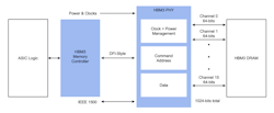
Now onto the improvements with HBM3 over HBM2E. To start, HBM3 brings significant performance increases over its HBM2E predecessor. With data rates of up to 6.4 Gb/s per data pin (Rambus is at 8.4 Gb/s) and an interface that features 16 independent channels, HBM3 can achieve 820 GB/s of bandwidth (close to 1 TB/s with a single HBM3 stack). That’s almost double HBM2E, which maxed out at 461-GB/s bandwidth.
HBM3 also will increase the supported DRAM chip capacity, increase the supported height of the 3D stack, and increase the data rate for higher bandwidth. Simply put, you can achieve up to 3.2 TB/s of bandwidth utilizing four HBM3 DRAM stacks.
The next difference between HBM2E and HBM3 is the increased power efficiency with HBM3. Specifically, IO voltage was dropped to 0.4-V low-voltage-swing terminated logic (LVSTL) IO for HBM3 (HBM2E and HBM2 are 1.2 V) to offset the greater power dissipation that comes with operating at higher speed. However, lower operating voltage reduces design margin, so gain in power efficiency comes at the cost of higher SI design complexity. Nevertheless, for all things computing, we’re always burning more power for greater performance, while trying to mitigate the increase as much as possible.
Lastly, although there have been many improvements from HBM2E to HBM3, the reliability, availability, and serviceability (RAS) of both solutions remains comparable. This is one of those instances where all of these improvements were introduced to offset the higher bit error rate and other inefficiencies introduced by operating at a higher data rate. Thus, HMB3 doesn’t necessarily get better RAS, but it’s able to maintain the same level of RAS at a higher speed.
Given the unrelenting need for higher bandwidth, HBM3 will take a commanding share of HPC and AI/ML applications before we know it. Companies will continue to demand faster and more powerful applications to scale their performance and one-up the competition. With the capacity and bandwidth benefits of HBM3, it’s clearly the new frontrunner.

