Vision DSP Family Eyes Low- and High-End Apps
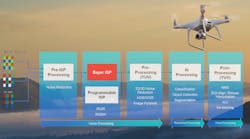
Cadence has experienced great success with its Tensilica Vision DSP family. The Tensilica Vision DSP family shares a common single-instruction multiple-data/very-long-instruction-word (SIMD/VLIW) architecture (Fig. 1). Its latest announcement is an expansion of the family of processor IP cores.
The company’s latest low-end solutions target applications like smart sensors, mobile devices, and augmented reality (AR), where low power and always-on are becoming more common. Features like user authentication via voice commands, face detection, and fingerprint recognition requires artificial-intelligence/machine-learning (AI/ML) support. High-end solutions analyze multiple video streams in real-time, and they also use multiple AI/ML models.
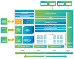
The SIMD/VLIW architecture includes multiple, wide, 2048-bit, dual load/store memory interfaces and scatter-gather support. The cores also feature a 128-/256-bit AXI iDMA interface.
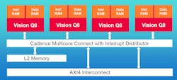
The Vision DSP family adds the new Tensilica Vision P1 at the low end and the multicore Tensilica Vision Q8 at the high end (Fig. 2). The Tensilica Vision P1’s 128-bit SIMD support can deliver over 0.256 TOPS of performance using one-third the area and power of its Tensilica P6 sibling. This make the P1 ideal for always-on applications that require minimal power.
The single-core Tensilica Vision Q8 supports a 1024-bit SIMD engine with 3.8 TOPS of performance and 129-GFLOPS FP32 floating-point performance. That’s twice the performance of the Q7 DSP.
This family of DSP cores provides developers with a range of options to meet different power and performance requirements that can include always-on, low-power solutions to high-performance, multistream machine-learning platforms. They share a common architecture and software solution from Cadence that allows for easy migration from one solution to another.
The company can provide developers with core IP or complete subsystems (Fig. 3). This is especially handy for more complex systems, especially those that need to address safety-related applications such as automotive platforms that need to be certified to safety standards such as ISO26262 ASIL-D certification.
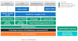
Cadence’s software support includes Halide, OpenCL OpenVx Graph, and C/C++ compiler support (Fig. 4). The runtime can work with its own single-threaded XTOS or multithreaded XOS operating systems or with third-party RTOSes. Software libraries are provided for features like TensorFlow Lite for Microcontrollers support.
The DSPs are supported by the Tensilica Xtensa Neural Network Compiler (XNNC). XNNC also can target Cadence’s AI/ML DNA 150 processor. XNNC supports AI/ML models from TensorFlow, Caffe2, Keras, PyTorch, and Chainer.
Floating point is optional in these platforms, where often integer or fixed-point support is sufficient for an application. The Tensilica DSP architecture handles all of the new compact, numeric formats used by AI/ML applications, especially when scaling down to reduce performance and power requirements. The high-end platforms include complex floating-point support for FP16, FP32, and FP64 data formats. There are ADDSUB FFT enhancements for FP16 and FP32 as well.
In addition, Cadence supports the Tensilica Instruction Extension (TIE) language. Designers can create new TIE instructions that are automatically handled by the optimizing compiler. Typically, these new instructions are hidden from high-level language programmers, with the compiler handling utilization and optimization of TIE instructions to deliver higher performance with less overhead. TIE instructions can be added while maintaining ISO26262 certification.


