What you’ll learn
- What is surrounding-gate-transistor (SGT) technology?
- How will SGT improve DRAM?
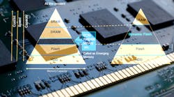
DRAM makes up the bulk of non-volatile memory in computer systems. Much has been done lately to mix non-volatile storage with DRAM. However, DRAM’s performance and capacity still win out when it comes to the processing units, including CPUs, GPUs, etc. The demand for more memory continues to push designers to using smaller geometries, but we’re starting to hit limits with the current capacitor-based solutions.
Unisantis has developed a surrounding-gate-transistor (SGT) technology that may give new life to DRAM. It would still employ a refresh approach like conventional DRAM, but reduced power leakage should allow further scaling to occur while improving performance and overall lower power requirements. Unisantis calls its new approach Dynamic Flash Memory (DFM) technology, though it’s not a non-volatile memory like NAND flash. Rather, it’s a technology aimed at DRAM without using a capacitive approach that’s applied to the current crop of DRAM implementations.
Planar and FinFET transistors make up the majority of storage and processor transistor technology at this point. Improved lithography has provided better performance, power, and area (PPA) utilization. The improved PPA has been offset by subthreshold leakage current, though (Fig. 1). This static leakage is the bane of mobile devices that run on batteries.
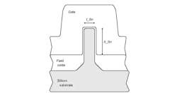
FinFET employs a vertical channel with a lateral current flow from drain to source (Fig. 2). The architecture effectively increases the width of the gate to boost drive current per unit area when the transistor is on. Improved electrostatic control also reduces the leakage current when the transistor is off. The process for creating new chips using FinFETs required enhancements to create a silicon fin with consistent sidewall slope and thickness.
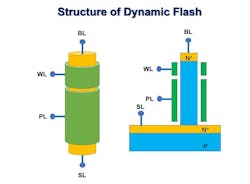
DFM’s 4F2 SGT is also vertically inclined like FinFET (Fig. 3). The main difference is that SGT surrounds the channel, whereas FinFET addresses three sides of the fin structure. The structure might look complex, but it’s actually easy to fabricate. It maintains a higher density than DRAM with very low leakage current and a long refresh period.
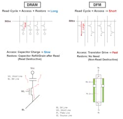
DFM delivers faster access times with longer refresh periods (Fig. 4). Conventional DRAM utilizes capacitors whereas DFM drives transistors. DFM reads also are non-destructive. A refresh cycle is still required, but less often, providing more bandwidth for normal reads and writes.
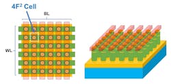
DFM arrays can be built using a basic cross-point structure (Fig. 5). The same approach is being used with high-density DRAM and flash memory.
DFM isn’t commercially available at this point. The inventors of DFM are Drs. Koji Sakui and Nozomu Harada from Unisantis. They presented the paper entitled “Dynamic Flash Memory with Dual Gate Surrounding Gate Transistor (SGT)” at the 13th IEEE International Memory Workshop this year.
