Companies specializing in circuit board and system design-for-test (DFT) tools are pursuing a variety of strategies to serve test and debug applications based on innovations they announced over the summer. In many cases, they continue to build on the boundary-scan and JTAG innovations but at the same time are furthering their embedded test technologies. The result is new general-purpose boundary-scan controllers as well as component-specific and embedded test tools that go by names such as embedded instrumentation or embedded system access.
Boundary-Scan Controllers
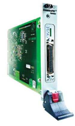
On the controller front, JTAG Technologies announced an extension to its line of boundary-scan IEEE 1149.1 controllers (Figure 1) in August. The new unit—the DataBlaster JT 37×7/PXIe—offers support for the PXIe/CompactPCI Express slot format that now features in some of the latest ATE based on the PXIe standards. The new product is intended to satisfy the growing requirements for high-speed in-system programming (ISP) of flash memories, serial memories, and CPLDs as well as complex digital circuit testing.
Courtesy of JTAG Technologies
The DataBlaster JT 37×7/PXIe features sustained test clock speeds of up to 40 MHz by use of JTAG Technologies’ proprietary Enhanced Throughput Technology (ETT) system. It also offers an onboard flash image buffer memory.
Peter van den Eijnden, JTAG managing director, said he sees more advantages as the JTAG capability is finding its way into many industry sectors, from automotive through to particle physics, several of which have demanding functional test requirements. Matching JTAG’s digital and mixed-signal hardware to their preferred environment is a priority for JTAG Technologies, he said.
ASSET InterTech also is extending its controller line. In May, the company introduced two controller kits for its ScanWorks platform for embedded instruments. The controllers can plug into the PCI Express (PCIe) bus in the PC on which ScanWorks is running, enabling the application of ScanWorks nonintrusive board tests (NBT) to a circuit board.
The PCIe-1000 is a single test-access-port (TAP) controller used for JTAG testing. The PCIe-410 controller kit has a four-port interface pod and can test as many as four circuit boards simultaneously. Both the PCIe-1000 and the PCIe-410 controllers also can program memory or logic devices that already have been soldered to a circuit board.
SPI Adapter
In August, Corelis announced the BusPro-S, a high-speed multi-IO SPI host adapter. The BusPro-S USB-powered desktop instrument allows engineers to save development time by providing low-level control of serial peripheral interface (SPI) buses for the generation of SPI messages and programming SPI memory.
Features of the BusPro-S include 60-MHz clock rates with up to 200-Mb/s throughput; standard, dual, quad, and 3-wire mode support; user-selectable interface voltages down to 1.8 V; eight independent slave select signals; a graphical user interface with a complete command script editor; and a royalty-free application programming interface (API).
The BusPro-S is controlled by the included SPI Exerciser software using two modules: Debugger and Programmer. The Debugger module features a command script interface with individual tabs for concurrent command sessions. All communications from the Debugger module are recorded and displayed in a detailed transaction log. The Programmer module enables fast, convenient in-system erase, program, verify, and read operations for both standard and multi-IO nonvolatile memory components using an included library of common flash and EEPROM device models.
Semiconductor Vendor Support
In other news, ASSET InterTech has leveraged its eight-year relationship with Intel to provide designers of micro-server circuit boards based on the Intel Atom processor with a tool capable of nonintrusively validating the signal integrity on high-speed input/output (HSIO) and memory buses. ASSET reports its ScanWorks platform for embedded instruments is the first design-validation tool for Intel Atom designs that does not rely on placing a physical probe on a bus to monitor its signal integrity.
Over the last eight years, Intel and ASSET have collaborated on validation and test tools that deliver visibility of the signal integrity on high-speed buses to overcome the shortcomings of legacy intrusive probe-based test equipment such as oscilloscopes and logic analyzers. Because buses with speeds in excess of 5 Gb/s become sensitive to capacitive coupling effects, the signaling on these buses is distorted when a physical probe is placed on them. To counteract this, Intel developed and is implementing an instrumentation technology embedded in its advanced chips. ASSET’s ScanWorks HSIO for Intel Architecture (IA) is a nonintrusive software-based toolkit to take advantage of Intel’s embedded instrumentation technology.
Other semiconductor vendors gaining support from DFT firms include Cypress, Freescale, and Xilinx. In June, Corelis announced that its free Runner-Lite test executive now is compatible with Freescale USB TAP probes. This added support allows existing Freescale hardware users to execute pregenerated JTAG-based test procedures on select Freescale reference designs. In conjunction with adding Freescale hardware support, Corelis has distributed a downloadable test procedure for the Freescale QorIQ P1024 reference design board.
Also in June, GOEPEL announced that, in cooperation with Xilinx, it had developed a new software option to support Xilinx’s Platform Cable USB II. The new solution integrates the Xilinx hardware into GOEPEL’s SYSTEM CASCON IEEE 1149.x development environment, enabling the utilization of Platform Cable USB II as native controller to execute boundary-scan tests throughout the entire product life cycle.
Similarly, in August GOEPEL announced that, in cooperation with Cypress, it developed a dedicated VarioTAP model library for the PSoC3 programmable system-on-chip series. GOEPEL describes VarioTAP as a universal processor-centric emulation technology for programming, test, and design validation. The libraries are structured modularly as intelligent IP, enabling a complete fusion of programming and test via processor debug interfaces and other technologies such as boundary-scan or chip-embedded instruments on a single platform.
VarioTAP enables the reconfiguration of the integrated processor into a native design embedded test and programming controller via the JTAG debug port. The IP contains all necessary functions to control the entire execution and for matching the stringent timing requirements. Accordingly, the use of VarioTAP does not require expert background knowledge, additional development tools, or processor-specific pods, which makes the handling easy and uncomplicated.
Complementing Traditional Test
In addition to working with semiconductor vendors, DFT companies also have been working to augment traditional instrumentation. In April, for example, Corelis introduced its QuadTAP/CFM, a four-channel JTAG hardware platform that integrates boundary-scan test capabilities into Teradyne in-circuit testers. The QuadTAP/CFM is designed specifically for use with Teradyne TestStation and GR228x Series testers. And in May, Teradyne confirmed that it has entered into an OEM agreement with Corelis to sell and distribute a package of Corelis ScanExpress boundary-scan test execution and diagnostic software and hardware modules.
In June, GOEPEL announced an enhanced OEM cooperative initiative with Rohde & Schwarz regarding the R&S TSVP (Test System Versatile Platform), which allows the execution of in-circuit and functional tests. Under the initiative, users can combine functional/in-circuit test and boundary-scan test to achieve a higher test depth and test speed. An interactive ATE function within GOEPEL’s SYSTEM CASCON supports automatic generation of interactive tests with sequential wiring on the R&S TS-PMB tester matrix.
Furthermore, users now have access to test and programming technologies such as processor-emulation test, FPGA-assisted test, and core-assisted programming.
iNEMI Memory Test Initiative
A key focus of ASSET InterTech has been memory test. ASSET’s new memory-test instruments are an effort to address issues identified during an ongoing research project conducted by the International Electronics Manufacturing Initiative (iNEMI) to investigate built-in self-test (BIST). iNEMI has found that the capability to test onboard memory was one of the two most pressing needs for electronics manufacturers.
In phase 1 of the project, iNEMI conducted a survey on BIST availability, usage, and access at board-level test. In phase 2, the organization investigated and specified use-cases to serve as discussion, modeling, and development material, and it identified main users of board BIST while defining board BIST and evaluating its value-add.
Phase 2 listed as use-cases the capability of BIST to test the interfaces between two adjacent ASICs and from an ASIC to external memory interfaces. These two use-cases form the focus for phase 3 work currently underway.1 Phase 4 will develop board-level test recommendations for standardization of component BIST.
Al Crouch, co-chariman of the iNEMI BIST Program, said, “We asked manufacturers what test problem they would like to have solved by BIST or embedded instruments, and they put testing soldered-down memory right at the top of the list along with high-speed I/O validation.” Crouch, who also is the chief technologist for core instruments at ASSET, added, “The participants in our research said they expected a big cost savings and better failure, debug, and diagnostic information when they had the ability to test memory with BIST mechanisms and embedded instruments rather than external testers. In fact, a related iNEMI study found that the capability to test soldered-down memory was a crisis in waiting.”
ASSET recently published a white paper authored by Crouch that noted several factors contributing to the memory test problem, including the disappearance of test pads and restrictions on placing test probes on memory buses because of capacitive signal distortion the probes could create.2 “Fortunately,” Crouch wrote, “there are a number of NBT or probe-less methods for testing memory, including boundary-scan test (BST), functional test, processor-based testing methodologies such as processor-controlled test (PCT), FPGA-based testing mechanisms such as FPGA-controlled test (FCT), and embedded memory built-in self-test (memory BIST).”
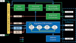
To address memory test, in August ASSET InterTech added two memory test instruments (Figure 2) to its ScanWorks embedded instrumentation library for its FCT circuit-board test tool. The new instruments, which ScanWorks FCT can temporarily or permanently embed in a functional FPGA on a circuit board, include a DDR2/DDR3 memory link test instrument and a generic memory tester. After engineers have selected as many instruments as they need to implement their NBT test strategy, ScanWorks FCT automatically configures, inserts, operates, and subsequently removes the FPGA-based board tester.
Courtesy of ASSET InterTech
This tester-in-a-chip can be employed during design to accelerate the board bring-up process by validating early prototypes before firmware and software are available, during manufacturing to ensure the quality of assembled boards, and later as a troubleshooting tool in field service. After it has been used, the ScanWorks FCT tester can be quickly removed and the FPGA’s functional firmware loaded.
SCANFLEX I/O Module
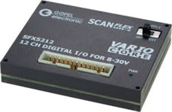
In August, GOEPEL electronic introduced the SFX5212 (Figure 3), another I/O module for the company’s SCANFLEX boundary-scan hardware platform. The new SCANFLEX module family member provides independently programmable I/O channels and processes voltages up to 30 V. Additionally, it offers VarioCore technology for dynamic configuration of module-specific FPGA based functions. Utilizing the SFX5212 provides users the opportunity to increase test coverage for non-boundary-scan circuits or peripheral signals with higher signal voltage by combining structural and functional test procedures on a single platform. In addition to increasing test quality, test costs can be reduced by saving separate process steps.
Courtesy of GOEPEL electronic
In cooperation with selected partners of its GATE (GOEPEL Associated Technical Experts) alliance program, GOEPEL has developed an API for SCANFLEX. The API provides third parties direct access to and control of the entire SCANFLEX hardware, down to the bit level, from their respective software systems. With this capability, users will be able to define synchronized interactions with other processes and modules as well as control non-JTAG protocols and hardware.
The new SCANFLEX API provides access to both serial TAPs and to all I/O modules, which can be controlled in parallel and independent from the TAPs. Using standard programming languages such as C/C++, Pascal, or Visual C, customizable serial or parallel vectors to be processed by the SCANFLEX hardware can be generated (and responses can be analyzed) by third-party software. Applications range from controlling special boundary-scan components, emulation sequences, and exotic programming tasks up to complex analysis functions for chip validation.
GOEPEL’s technology development efforts are informed by what the company calls embedded systems access (ESA).3 Thomas Wenzel, managing director of GOEPEL’s JTAG boundary-scan division, and Heiko Ehrenberg, technology officer for ESA, have identified three principle access strategies: native connector access through design-integrated I/O interfaces, intrusive board access through physical test nails and probes, and embedded system access through a design-integrated test bus. They propose a nonmutually exclusive combination of boundary-scan test, processor-Emulation Test, chip-embedded instrumentation (via IJTAG IEEE P1687), ISP, core-assisted programming, FPGA-assisted test, FPGA-assisted programming, and system JTAG as well as other technologies and standards such as the so-called on-chip emulation for software validation.
Wenzel and Ehrenberg summed it up succinctly: “The trend of employing noninvasive test access strategies, initiated in 1990 with the ratification of IEEE 1149.1, has spawned a number of new technologies and methodologies, which combined, have given birth to the category of ESA techniques. The essence of ESA is the provision of test-pin electronics in the target system itself. Activating ESA results in a temporary transformation of the respective system, allowing it to be tested in partitions by embedded test centers under control of the integrated test bus.”
References
1. “Built-In Self-Test (BIST) Project, Phase 3: Short-Term and Long-Term Strategies for Use Case Standardization,” iNEMI, Statement of Work, July 17, 2012.
2. Crouch, A., How To Test High-Speed Memory With Nonintrusive Embedded Instruments, ASSET-InterTech, White Paper, 2012.
3. Wenzel, T. and Ehrenberg, H., Embedded Systems Access (ESA): Changing the Paradigm of Electrical Test, GOEPEL electronic, White Paper, 2012.
For More Information
ASSET InterTech
Corelis
GOEPEL electronic
JTAG Technologies
Rohde & Schwarz
Teradyne


