The proliferation of semiconductor devices into safety-critical applications such as automotive and medical opens a new can of worms for test and reliability. An ever widening range of devices must achieve stringent test and reliability levels defined within new semiconductor safety standards such as ISO 26262 and IEC 61508. In concrete terms, these parts must undergo manufacturing testing that will ensure two key requirements:
- very low DPM (defects per million) levels and
- support for an in-field test capability to monitor any degradation over time.
In the past, these two test requirements have tended to be addressed by separate solutions, but perhaps a better approach is to combine leading solutions in both ATPG (automatic test pattern generation) compression and logic BIST (built-in self-test). A hybrid test solution recognizes that much of the circuitry and test-vector generation required for each type of test is similar and can be combined into a single DFT (design for test) flow and integrated circuit design. The hybrid test approach can reduce test cost and chip real estate, save developer time, and reduce time-to-market.
Scan-test evolution
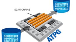
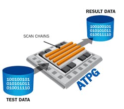
Scan-based ATPG testing has been around for many years and is still the most common methodology for testing the logic portion of a device. In scan-based ATPG, flip-flops throughout the logic are connected when in test mode into a number of serial shift registers, referred to as scan chains, so that test pattern data can be loaded into the flops using a serial scan process. After each scan load, the test data is applied to the functional logic and the response data is captured into downstream flops and then the scan process is once again used to unload the test response data. The basic scan ATPG setup is illustrated in Figure 1.
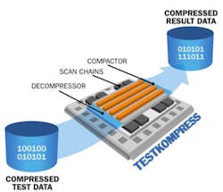
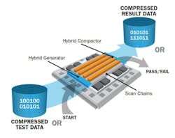
The time to test a device is proportional to the amount of test data that is applied, which in turn is proportional to both design size and the number of defect types that need to be covered. Of course, design sizes and complexities have grown exponentially following Moore’s Law, and consequentially ATPG test times have seen similar growth. It became clear several years ago that ATPG had to become much more efficient in order for test costs to remain economical. This powerful need for more economical test drove the development of ATPG compression technology. In this more advanced approach, the test data is compressed into a much smaller volume. This is possible because only a small portion of the bit values loaded into the scan chains are actually required to perform the desired test. Only the compressed test data is stored on the external tester and applied to chip pins. On-chip circuitry is added to intercept and decompress this data before streaming into the device’s scan chains. The basic ATPG compression setup is illustrated in Figure 2.
On-chip logic is also added on the output of the scan chains to compact the test responses before unloading back to the tester. ATPG compression reduces both test data volume and test application time. The volume reduction is important because it limits ATE memory requirements and related costs. In particular, ensuring that all test patterns can fit into the tester’s existing memory is critical, since the cost to reload the tester with additional patterns at each device insertion is prohibitive.
The reductions achieved in test time with ATPG compression are generally even more important because they are directly correlated to test cost per device. Leading-edge ATPG compression technology can generally achieve 100X compression. For many designs the level of compression can be even higher, sometimes approaching 1000x.
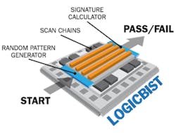
Despite these drastic ATPG improvements, test-pattern volumes continue to increase along with the increasing design sizes. One test approach that is effectively immune from these growth issues is logic BIST. This technique is based on generating random test data and analyzing all test responses on chip and therefore requires no test data storage whatsoever. The basic BIST setup is illustrated in Figure 3.
The test coverage achieved with random patterns follows a logarithmic curve with the knee in the curve generally occurring between 80% and 90%. The most practical way to achieve the remaining coverage is to insert test points throughout the design. Test points consist of local modifications to the netlist designed to increase the controllability or observability of a given net. Even with test points, however, full coverage may require test times equal to or greater than the test times of ATPG. Logic BIST also requires more stringent design rules than those required for ATPG. In particular, unknown circuit states cannot be tolerated, as these would corrupt the analysis circuitry used to compressed test response data into a final signature. Because of the constraints in coverage and design requirement, logic BIST has been used mainly for in-system test-related applications where the storage of patterns is difficult or impossible, and where fault coverage requirements are less stringent than for manufacturing test.
Why use a hybrid test solution?
Although ATPG compression and logic BIST solutions have historically been used independently and for different applications, they possess complementary features that turn out to be very beneficial in combination. The two solutions also make use of much the same on-chip DFT resources. They both make use of scan chains and related test clocks, and both benefit from maximizing the number of these scan chains, which maximizes test application bandwidth and thus minimizes test time. Both solutions can be integrated into a design using much of the same flow automation capabilities. Common features include, for example, design rule checking, scan insertion, and fault simulation.
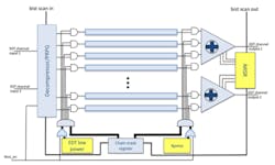
The main difference between the two solutions lies in the on-chip logic feeding test data to the scan chains and processing the test response data coming out of the scan chains. It turns out, however, that there are also similarities in this logic so the logic of the two solutions can be effectively combined to support both approaches. A diagram illustrating the overall architecture for the hybrid solution is shown in Figure 4.
All on-chip resources shown in blue are common to both test approaches. Only the few resources shown in yellow are unique to one approach or the other. The overall architecture, shown in Figure 5, provides the ability to apply any combination of compressed patterns and random patterns.
One of the benefits of this hybrid approach is greatly improved test efficiency during manufacturing test. Random patterns can be applied first to cover the faults that are easier to detect. The tester storage can then be more effectively used to store ATPG compressed patterns that cover the more difficult-to-detect faults. This top-up approach improves the overall coverage achievable with the available tester storage.
The hybrid solution can also reduce the total test time for a complex hierarchical design. In a hierarchical DFT implementation, each core is equipped with an independent set of scan chains, test clock control, hybrid on-chip test logic, and isolation scan cells on the periphery so that the core can be tested independently of other cores on the chip. This independence allows any combination of cores to be tested in parallel, thus reducing overall test time.
Consider, for example, a design with four cores. If an ATPG compression-only strategy is used, then the four cores must share the available tester pattern application bandwidth. The two typical scenarios would be to either test each core sequentially using all available tester channels for each core, or test all four cores in parallel with the tester channels distributed in some fashion across all four cores. However, if each core has both ATPG compression and logic BIST available, then the test for each core can be divided into two phases—logic BIST in one phase and ATPG compression in the other—to implement the top-up approach described earlier. With this separation, the entire chip can be tested in two phases. In the first phase, as an example, logic BIST is used to test two of the cores while ATPG compression is used to test the remaining two cores. In the second phase the situation is reversed. The advantage now is that in each phase, only two cores are sharing all available tester channels, as logic BIST does not require patterns from the tester. This means the bandwidth to each core is doubled thereby reducing the test time by half.
In addition to achieving greater efficiency during manufacturing test, the logic BIST portion of the hybrid solution is perfectly suited to supporting a power-on self-test (POST) capability. The ability of a device to automatically test itself when first powered on is a necessity in many safety-critical applications, and is a key to satisfying the reliability requirements specified within the ISO 26262 automotive safety standard.
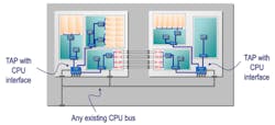
The logic BIST capability can also be combined with other on-chip test capabilities such as memory BIST to provide in-system test coverage for most, if not all, of the design. All BIST capabilities can typically be accessed through a standard IEEE 1149.1 Test Access Port (TAP) controller interface. However this dedicated interface is normally used during manufacturing test and is often not accessible in-system. One existing approach to accommodate in-system access is to enhance the TAP controller to also support a generic CPU interface that translates between parallel read/write CPU operations and the serial bit sequences required by the TAP protocol. This interface IP and supporting automation enables any external CPU or embedded CPU core to communicate with all the BIST capabilities through any internal system bus. This is illustrated in Figure 6.
The CPU read/write commands that are needed to initialize and execute any BIST capability can be stored into any CPU-accessible memory. For situations where a fully autonomous POST capability is required, a fairly simple finite-state machine based test controller can instead drive the TAP controller. When activated by a power-on reset signal, this test controller automatically applies the necessary serialized sequences to the TAP to perform any needed BIST initialization and activation.
Maintaining cost effective test in the face of growing design sizes and complexity requires improvements in test efficiency. The new hybrid solution described here combines the benefits of both ATPG compression and logic BIST, delivering not only significant efficiency improvements but also addresses the emerging requirements for in-system test required by the rapidly growing number of designs targeted for safety critical applications.
About the author
Steve Pateras is product marketing director within Mentor Graphics Silicon Test Solutions group and has responsibility for the company’s ATPG and DFT products. He received his Ph.D. in Electrical Engineering from McGill University in Montreal. [email protected]
Additional reading
Pateras, S., “Test Innovations for ISO 26262,” EE-Evaluation Engineering Online, Jan. 30, 2014.
