GPU Software Brings New Level of Speed to Fab Chip Design
NVIDIA is one of the world's largest fabless chip firms, using foundries and other third-party companies to fabricate and package its high-end GPUs instead of maintaining its own chip-making operation.
Now, the Santa Clara, Calif.-based company is giving back to the semiconductor ecosystem that helps power its business. NVIDIA has launched cuLitho, a software library that runs all parts of a computational lithography process in parallel on its latest GPUs. The software is claimed to give fabs 40X faster performance at a fraction of the power when it runs on its latest “Hopper” GPUs instead of CPUs.
CEO Jensen Huang said the innovation is important as modern chips become more complex due to the larger number of transistors in newer nodes and manufacturing costs for high-end chips continue to rise.
As the likes of Intel and TSMC race to roll out 5-nm, 3-nm, and even smaller process technologies, it’s no longer sustainable for companies to operate the way they did before Moore’s Law started to slow down. For years now, semiconductor fabs have turned to computational lithography to transfer the transistors, wires, and other building blocks of a modern processor onto a silicon wafer faster and more accurately.
Computational lithography is one of the most intensive workloads in chip design and manufacturing. It requires vast data centers that run behind the scenes 24/7 at fabs and, thus, expend vast amounts of electricity.
Last month, at GTC 2023, Huang explained that cuLitho can reduce the development cycle for any foundry using it, pushing the pace of innovation the world has come to expect from the semiconductor industry.
Long term, NVIDIA said it could lend a hand in creating smaller, more advanced process technologies—ones that it can use, in turn, to cram more computing power into its GPUs than what’s possible nowadays.
Behind the Mask
Every chip design these days is composed of about 100 layers that contain in total trillions of polygons, patterns, and other shapes that represent the building blocks of the transistors and other features inside a chip. Each one of these layers is portrayed on a template of the chip’s design—called a photomask—used by a fab in the manufacturing process. During lithography, a beam of light shines through it to sear the outline of the transistors on a silicon wafer.
Upgrading a chip to a smaller, more advanced process node requires the foundry to update the templates used to produce it. For decades, these masks resembled a stencil of the processor to be scorched on the silicon wafer.
Today, the components inside a modern chip are bundled so tightly together that these templates rarely resemble the final product at all. The scale of the transistors and other building blocks at more advanced process nodes also can distort the final chip’s design when light is beamed through the masks. If left unchecked, the arrangement of the transistors and other features of the chip will remain blurred.
Computational lithography is used to bring everything back into focus. By sharpening the shape and dimensions of the holes in a mask, it enables fabs to etch smaller transistors on the surface of a silicon chip and cram them all closer together.
The types of computational lithography in use today include corrective optical proximity (OPC) and inverse lithography technology (ILT). ILT is the more advanced of the two, but it’s more computationally expensive, too.
As these templates become more intricate, a greater amount of computational horsepower is required to build them. That translates into tens of thousands of servers that use general-purpose CPUs to take care of computational lithography.
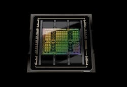
NVIDIA said its H100 GPU, based on its “Hopper” architecture, requires 89 masks to be manufactured. When using general-purpose CPUs to run computational lithography, it takes up to half a month to create each one.
On the other hand, when using cuLitho coupled with Hopper GPUs, NVIDIA said it would take only eight hours to process the same photomask.
Unlike other parts of the chip design process, AI is not yet playing a part in computation lithography. But the company said it could add AI to cuLitho in the future to boost chip design and manufacturing speeds further.
The Future of the Fab
NVIDIA is partnering with key players in semiconductor design and manufacturing to adopt the new tools. For instance, chip-equipment maker ASML is integrating support for GPUs into its software for computational lithography. Electronic-design-automation (EDA) giant Synopsys is bringing cuLitho to its software and systems, too.
Along those lines, TSMC is integrating the software library into its foundry operations to improve its production of photomasks. It has the potential to boost both the output and yield of the company’s facilities, thus reducing costs per chip over the long term.
Using cuLitho, NVIDIA said semiconductor fabs can create 3X to 5X more photomasks per day, which could significantly improve time-to-market for a new generation of GPUs and other ICs.
cuLitho also is a boon when it comes to reducing the amount of power used to do computational lithography. As a bonus, the power savings promise to reduce the carbon footprint of the colossal data centers where such workloads run.
NVIDIA said 500 of its DGX supercomputers with 4,000 Hopper GPUs can match the performance of 40,000 CPU-based servers when using cuLitho for computational lithography, reducing the power required from 35 to a mere 5 MW.
Furthermore, cuLitho could help pave the way for other innovative technologies. One such technology is the High-NA EUV system, which the world’s top semiconductor firms are counting on to help them fabricate more advanced chips, according to NVIDIA.
“Our collaboration with NVIDIA on GPUs and cuLitho should result in tremendous benefit to computational lithography, and therefore, to semiconductor scaling,” said ASML CEO Peter Wennink.


