AI Lends a Helping Hand with Analog and Custom IC Design
Skilled engineers remain the driving force for innovation in chips. But it’s no secret that electronic design automation (EDA) companies are folding AI into more of their offerings to speed up design and verification.
But as industry insiders tell it, these AI-powered EDA tools don’t have enough intelligence to actually replace human designers anytime soon. Instead, the biggest difference these tools are having is on the productivity front, with AI reducing the number of hours that engineers spend on the more tedious phases of the design and verification process, said Amit Gupta, VP and GM of Siemens Digital Industries Software's custom IC verification division.
Specifically, three main types of AI are becoming prevalent in the world of EDA. The most mature are what he calls “adaptive AI,” which enhances existing EDA processes to cut down on manual labor, and “additive AI,” which learns over time to save engineers from repetitive work. Further along on the roadmap is “assistive” AI. It can pinpoint weak points that can negatively impact the chip design’s performance and then figure out the root cause.
While these technologies are all at varying stages of development, they all play a part in Siemens’ newly released Solido Design Environment, the latest addition to its intelligent custom IC design and verification platform.
Siemens said Solido Design Environment can be used throughout the design process to set up Spice-level simulations for circuit measurements and regressions as well as view waveforms and analyze statistical results on standard cells, memory, analog, and other custom IC designs. Everything is accessed from a single cockpit that handles nominal and variation-aware analysis.
Solido brings AI into the fold to help customers identify “optimization paths” to improve circuit power, performance, and area (PPA), as well as to perform production-accurate verification with significantly faster runtimes.
Why EDA Tools Need AI
It’s a constant challenge for engineers to adapt to the higher design complexity and increasing variability and parasitics present in modern chips, while balancing tradeoffs in PPA and cost. Chips also need to be tested at more temperatures, voltages, and other corner cases that can ruin chips—and cut into yields—if you’re not careful. All of these variables translate to more time being spent on IC design and verification.
Using AI, and specifically machine learning, is one way to close the productivity gap, said WeiLii Tan, principal product manager at Siemens EDA. But it’s important that the AI at the heart of EDA tools is “industrial grade” since the consequences of the technology giving out incorrect or even slightly inaccurate results can be dire.
Tan pointed out that “the AI needs to be highly accurate. It needs to give you the same results that traditional methods would have given you, while it allows you do everything much faster, with much faster runtimes.”
“The sheer amount of resources needed to design a chip—and the cost of making mistakes or producing non-functioning or non-spec silicon—is huge,” said Tan, citing estimates that the upfront cost for designing a 5-nm chip can reach up to $550 million.
And unlike consumer AI models that sit in the cloud and are used by a company’s entire customer base, it’s vitally important the AI models inside EDA tools remain under a semiconductor company's immediate control.
One of the features of the Solido Design Environment is that it automatically produces custom AI models that are stored inside the tool, said Gupta. That way, the most valuable data about a company’s proprietary designs—the “crown jewels” of any semiconductor maker, as he called them—is protected. The AI models are specific to the customer, their designs, their measurements, and even the foundry that they work with.
AI Adapts to the Situation
Siemens is applying adaptive AI in the Solido Design Environment to reduce the time it takes to simulate and verify that analog, mixed-signal, and other custom IC designs work as intended and meet system-level requirements.
Whether under the hood of a car or plugged into a data center, custom IC designs need to be as close to perfect as possible. In many cases, they must be rigorously tested to the point called “6 sigma,” where failures are a one-in-a-billion occurrence. But modern chips are so intricate that it can take up to tens of billions of simulations at the transistor level to find and fix every weakness. A brute-force approach is not cutting it anymore, said Tan.
Solido applies AI to chart a shortcut through the verification process. Customers input all of the same data that they usually plug into Spice simulation tools, and Solido uses the data to automatically build a custom machine-learning model. Then, the AI intelligently figures out what samples to choose and what tests to run so that it can make accurate conclusions on the reliability and quality of the chip design, said Siemens.
The AI continuously plots additional points to verify that its assumptions are correct. Before finishing, it runs real simulations to make sure that it’s capturing all of the points in the IC design with a high risk of failure.
“This type of AI optimizes the engines underlying the EDA tools to improve performance, so it’s AI that allows the software to significantly reduce the number crunching time that’s required,” Tan told Electronic Design.
The result: more accurate verification without having to run as many computationally intense simulations. Siemens said Solido Design Environment supports the same level of design coverage as tens of trillions of simulations, but it only needs to run several thousand simulations to do so.
“It’s a superpower for designers,” said Gupta, adding that this type of AI has been at the heart of its Solido offerings for years and is being used by thousands of engineers today. “They can use AI to boost the value of every simulation that they’re doing.”
AI Adds to What It Knows
Designing and verifying a chip is a highly iterative process, and semiconductor firms rarely get everything right the first time. They tend to run through several different permutations of a chip design or layout over time, fine-tuning the lengths and widths of the transistors to meet the specifications set out at the start of a project or adapt to new requirements. Foundries are constantly adjusting the process node used to fabricate the final chip, too.
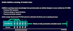
To save time, Siemens said Solido Design Environment can reuse AI models that it created at other points in the design process to help speed up subsequent verification runs, reducing runtimes by 10X to 100X.
For instance, companies that intend to use the most advanced process nodes in the pipeline usually start plotting out analog or other custom IC designs years before the process even moves into mass production. While a company works out its latest SoC or IP block, the foundry it intends to use—or that its customers prefer—is making gradual improvements to its process technology. “Everyone wants to be out the door as soon as possible,” explained Tan. “The design process can’t always wait for the process node to mature.”
A process design kit (PDK) is a set of files used within the semiconductor industry to model a manufacturing process for the EDA tools used by engineers to design, simulate, and verify a chip design in pre-production. If you’re designing a chip based on a process still in development, such as 3 nm or 2 nm, the foundry sends a pre-release copy of the PDK for the process—call it, PDK 0.5—so you can start plotting out the IC design. But as the process matures over time, the foundry updates the underlying PDK—PDK 0.6, PDK 0.7, and so on—said Tan.
However, every time the foundry slightly changes the formula, you’re forced to run another set of simulations and re-verify the chip design. Each round of verification takes a fixed amount of runtime that gradually adds up.
Siemens said Solido uses “additive” AI technology to consider what it learned the first time through the verification process—with PDK 0.5—to reduce the runtime during the second round of simulations—with PDK 0.6. The tool can then reuse the AI models stemming from the verification process with PDK 0.6 to reduce the time it takes to verify the circuit design using PDK 0.7, and so on. “This is a game-changer,” claimed Tan.
He said the time savings can add up to weeks or even months of design and verification for chip companies.
AI “Assists” With IC Design
The final type of AI that companies are applying to EDA is what Siemens calls “assistive” AI. It’s designed to help boost the productivity of engineers by giving them deeper insights into the inner workings of their devices.
Using its AI functionality, Siemens said Solido Design Environment can sort through the vast amounts of data stemming from the design process and point out weak spots in the chip’s design where engineers are leaving some PPA on the table. The tool can also guide them to the transistors—and even the characteristics of the transistors—that are causing failures and then root-cause what went wrong.
The use of AI in EDA is still a work in progress. It will take further improvements to convince chip firms that it’s not only fast and accurate, but also reliable and verifiable enough to be used throughout the design process.
For its part, Siemens made a point of making the Solido Design Environment easy to use even for the average semiconductor engineer, keeping the technology as much as possible “under the hood,” said Gupta.
While still in the early stages, it’s clear that AI-powered EDA tools are here to stay.


