Sound-Card Signal Generator Interface Adds Variable Offset Control
A personal computer (PC) sound card can be the basis for a readily available signal generator for testing electronic circuits. The usefulness of these signal generators is limited, however, because their outputs are ac coupled and restricted to ±2 V.
Related Articles
- Simple Circuit Turns Scope, Function Generator Into JFET Curve Tracer
- Low-Cost Function Generator
- Function Generator Uses +5 V, Ground
This circuit takes advantage of the two channels provided by the sound card by using one channel to output the sine/square/triangle waveform with a fixed gain while setting up a 441-Hz pulse-width modulated (PWM) square wave on the second channel. This PWM waveform is converted to ±8 V, then averaged and summed with the first channel, to provide an adjustable dc offset that is controllable by the duty-cycle setting.
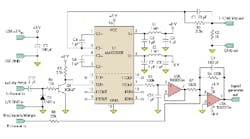
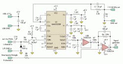
The circuit provides a variable offset of typically ±5 V at the signal generator output (Fig. 1). It is powered from the PC’s USB +5-V supply, which is converted by the capacitive voltage generator within dual driver/receiver IC U1 to ±8 V (typical) to power the low-power dual op-amp U2.
Passive pairs L1/C3 and L2/C8 filter out the ripple on the V+ and V– outputs of U1. The 441-Hz PWM waveform output on the sound-card left-channel is clamped by the C10/D1 combination and fed through R8 to the base of transistor Q1. This produces a TTL-compatible (transistor-transistor logic) square wave at the collector of Q1, which is fed to T2IN of U1.
T2OUT provides a ±8-V PWM waveform that is averaged by filter R5/C11 and buffered by U2B to generate a dc voltage depending on the PWM duty cycle. This voltage is summed along with the sine/square/triangle waveform output on the sound-card right channel by U2A, forming the signal-generator output.
The C9/R4 pair forms a low-pass filter to smooth the quantized signal generated by the sound card. With the values of the components shown, the right channel is amplified by a fixed gain of +5.5 and the dc offset variation is typically ±5 V.
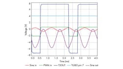
The 75% duty-cycle PWM input signal is converted to typically ±8 V at T2OUT and, when averaged, produces approximately 4-V dc at pin 7 of U2B (Fig. 2). The 0.5-V sine wave is amplified and offset by the inverting summing amplifier U2A to form the signal-generator’s output.
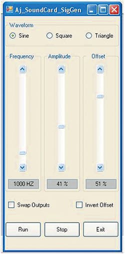
This design removes the limitations of ac coupling and the ±2-V signal level limit. It also provides a bonus output by dividing the output at U1 pin 3, using R1/R2 to provide a 1-V, 40-kHz square wave that can be used for step-response testing of analog circuits. Graphical user interface (GUI) software developed in VB.Net is also available here (Fig. 3).
Ajoy Raman (www.ajoyraman.in) is retired, having 37 years of R&D experience with the aeronautical development establishment in Bangalore, India. He has BTech and MTech degrees in electrical engineering from IIT Madras, India, and now pursues his love of electronics as a full-time hobby, with an emphasis on projects and low-cost teaching aids for students. He has received the Siemens prize for best academic record (M.Tech IIT, Madras), the Dr. V.M. Ghatge Award from the Aeronautical Society of India, and the DRDO Scientist of the Year Award. He can be reached at [email protected].


