Download this article in .PDF format
This file type includes high resolution graphics and schematics when applicable.
FGPAs are used in a large variety of applications, ranging from embedded computing to high-speed serial digital communications. With reconfigurable hardware and dense high-speed logic functions, they are ideal for implementing high-performance, flexible designs.
As part of their high-density architectures, FPGAs include internal integer and fractional phase-locked loops (PLLs) for frequency synthesis. This architecture leads to a simple question: to optimize performance and simplify design, when should an FPGA-based design use an internal PLL versus a discrete oscillator or clock IC?
Control Plane Timing
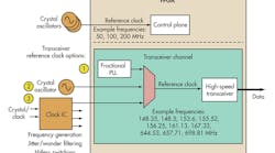
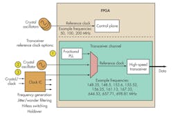
FPGA internal PLLs provide low-skew clock sources for functional blocks, including high-speed logic, digital signal processing, and embedded memory. They also are used to generate global and regional clocks and other high fan-out, low-skew control signals. External input reference clocks are required to drive these internal PLLs. Simple fixed-frequency oscillators are often used to provide these references (see the figure).
Developers should consider three key criteria when selecting an oscillator to provide FPGA control plane timing:
• Long-term reliability: FPGAs are typically used in applications that have long life cycles, which makes it important to ensure that all board-level components are rated for long-term operation. Oscillators are a key concern since quartz crystal-based components are responsible for the highest rate of field returns in many electronics applications. Crystals are susceptible to contamination issues that can affect startup and frequency drift over time and temperature. To ensure long-term reliability, developers should select oscillators that guarantee long-term operation. The appropriate oscillator should guarantee at least a 10-year operating life and specify lifetime aging at an accelerated temperature (e.g., 40°C or higher).
• Board-level noise immunity: FPGAs generally operate in noisy environments surrounded by switching power supplies. They also generate noise that affects VDD and ground planes. Minimizing this noise, which cannot be eliminated, can be relatively expensive. When selecting an oscillator, power supply noise filtering is an important consideration. Oscillators with internal power supply voltage regulation provide noise rejection, enabling more resilient operation by ensuring the device does not violate its stated jitter specifications when subjected to system-level noise.
• Availability: Oscillators can take significant time to procure due to the material-intensive, complex manufacturing process associated with quartz processing, die assembly, and packaging. Custom frequency oscillators can take even longer to obtain. Choose oscillators that are available for rapid, quick-turn delivery, either in stock at distributors or quickly programmable by the supplier. Fast component availability eases prototyping and enables a speedier design.
Alternatively, frequency-flexible clock generators are available to replace multiple crystal oscillators with a single IC. These highly integrated clocking solutions are recommended in FPGA designs that require multiple clock references.
FPGA Transceiver Clocking
In addition to reliability, power supply noise rejection performance, and availability, developers should consider other factors for FPGA-based transceiver clocking applications. For high-speed serial data communications (e.g., 10/40/100G Ethernet, Optical Transport Networking [OTN], 3G-SDI, CPRI, and PCI Express), reference clock selection is critical because clock jitter adversely impacts transceiver bit-error rate.
Complicating matters, multi-rate applications require a range of different reference frequencies. Hardware designers typically have three transceiver reference clock options:
• Internal integer or fractional PLL: High-performance FPGAs include internal integer/fractional PLLs that can be used for transceiver clocking. These PLLs offer the lowest jitter when operating in integer mode. When used for fractional clock synthesis, some jitter performance is sacrificed. While the jitter performance of this solution is acceptable for some applications, discrete oscillators and clocks can provide lower jitter and better optimize FPGA transceiver performance.
• Oscillator: Single-frequency oscillators are available for clocking fixed-rate applications. For multi-rate transceivers, I2C programmable oscillators that are serially programmable to a wide range of frequencies are a superior solution. One benefit of I2C programmable oscillators is they can be used in conjunction with an FPGA’s integer PLL. The oscillator can provide low-jitter fractional clock synthesis, and the FPGA’s internal PLL can provide further integer clock multiplication and low-skew clock routing.
• Clock generator/jitter attenuating clock IC: The highest-performance method for clocking multiple FPGA transceivers is to use a multi-output clock generator/jitter-attenuating clock. Frequency-agile clock generators can be used for clocking transceivers in addition to providing control plane clocking. A jitter-attenuating clock IC is required for applications that require synchronization, such as SONET/SDH, Synchronous Ethernet, broadcast video, and CPRI. These devices integrate ultra-low phase-noise voltage-controlled oscillators (VCOs) with a low-bandwidth PLL (0.1 Hz to 1 kHz typical) to provide jitter/wander filtering in addition to ultra-low jitter frequency synthesis. Jitter-attenuating clocks also provide hitless switching, which absorbs the phase difference between two input clocks during a switchover. This minimizes the risk that downstream low-bandwidth PLLs will lose lock due to a clock rearrangement. Finally, jitter-attenuating clocks provide a holdover reference clock function, ensuring transceivers maintain proper operation in the event the reference clock is not available. This mission-critical feature is essential for communications applications that require 99.999% availability.
Ultimately, it is up to hardware engineers to select the right combination of internal and external clocking solutions for their FPGA-based applications. Now more than ever, hardware designers have a wide range of timing choices to choose from to optimize their next design.
James Wilson serves as marketing director for Silicon Labs’ timing products, overseeing the marketing program for the company’s clock and oscillator products. He joined Silicon Labs in 2002 as a product manager focusing on optical networking solutions. Previously, he worked at Freescale Semiconductor’s networking and communications systems group in Austin, Texas. He holds a BS in mechanical engineering and a master’s degree in business administration from the University of Texas at Austin. He can be reached at [email protected].

