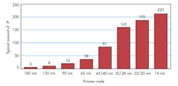
Today’s systems-on-chips (SoCs) integrate large numbers and varieties of intellectual property (IP) that come from multiple sources. Some are developed internally. Others come from one or more external suppliers. The integration of the Joint Test Action Group (JTAG) chains of these varied IP and their related controllability has proven to be a challenge that chip designers have either just accepted or have tried to address by using ad hoc solutions (Fig. 1).
Even if the large amount of IP is developed within a single chip-design company, there is the challenge of coordinating globally dispersed teams that are each working on a piece or block of the design. Each IP comes with its own built-in self-test (BIST) solution and its own JTAG connection to the outside world.
With I/Os at a premium, test ports are particularly expensive to replicate in pad-limited designs. Chip designers have made tradeoffs by dropping some other I/O or sacrificing test coverage or IP controllability. Alternatively, they have invested engineering resources to combine these different test chains to conserve die area and reduce the number of JTAG ports.
These ad hoc IP test integration approaches are based on in-house scripting and typically rely on direct access to I/Os. This may have been a viable solution in the past when the average design had a small number of IP whose I/Os could be brought out directly at the SoC level. But with larger designs, more IP, and a limited number of I/Os, direct testing of the entire design is not an option. Standard top-down design-for-test (DFT) approaches using centralized test management or control add area while increasing design time and test costs.
One possible solution is to use a hierarchical DFT approach with a standard and unified interface that enables efficient testing of large designs without adding area or additional test costs. Such an approach enables sign-off at each design hierarchy for integration at the SoC level. As different design blocks or hierarchies are completed in various parts of the world by different teams, each team can sign off on test in the same way it would sign off on timing or any physical aspect of the design. Then, the blocks can be integrated into a single unified design.
This file type includes high resolution graphics and schematics when applicable.
As design size increases, the test pattern development time and the amount of time required to test the entire SoC both increase significantly. It is not uncommon for designs to be over 100 million gates, requiring several weeks to develop chip-level test patterns. In such scenarios, it is useful to be able to reuse the test patterns at the IP or block level and then automatically port those patterns to the SoC level and test the entire SoC.
A Hierarchical Approach to SoC Test
An effective hierarchical test solution should provide an area-efficient and unified framework to control and observe the many IP blocks. It also should enable IP and block-level test pattern portability to the SoC level, eliminating the need to recreate them. And, it should use a well-understood standard as the interface to the IP to enable an ecosystem of support from both IP suppliers and test solution providers.
IEEE 1500 is just such a standard. This industry-defined scalable standard architecture enables test reuse and integration for embedded cores and associated circuitry. When used in conjunction with the widely popular 1149.1 JTAG standard, it provides a convenient solution to the challenge of hierarchical SoC test.
Also known as “Standard Testability method for Embedded Core-based Integrated Circuits,” IEEE 1500 includes serial and parallel test access mechanisms (TAMs) and a rich set of instructions suitable for testing cores, SoC interconnect, and circuitry. Core test language (CTL) is the official mechanism for describing IEEE 1500 wrappers and test data associated with cores.[1]
While it explicitly claims to forego addressing analog circuits and focuses on facilitating efficient test of digital aspects of SoCs, it can be used to interface with analog and mixed-signal IP. A standard like IEEE 1500 gives users the flexibility to utilize it in test and debug environments throughout the design lifecycle.
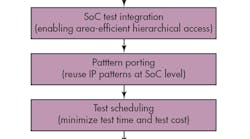
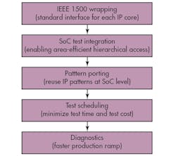
By leveraging IP or block-level diagnostics and providing SoC-level diagnostics, it can pinpoint exactly which test failed and where the failure occurred, which helps reduce the overall design and production ramp-up time. There are many steps in implementing a hierarchical SoC test solution: IP accessibility, SoC test integration of all the blocks, pattern creation, test scheduling, and post-silicon diagnostics (Fig. 2).
The IEEE 1500 standard is the de-facto standard for IP-based or core-based test. It provides a flexible means of interacting with each of the individual IP and digital logic blocks. Wrapping each IP block with a module that has an IEEE 1500 interface is the first step to improving accessibility and observability. Since it is an industry standard, a solution that leverages existing IEEE 1500 interfaces also enables a standard communication channel with all the IP and blocks from the SoC level.
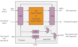
It is important to have a test solution that can create these interfaces with optional wrapper boundary registers (WBRs) for IP and blocks that don’t already have them. SoC designers could potentially create these wrapper modules with WBR registers that capture all the states of the underlying IP. However, this could lead to an unnecessary increase in area and power. As with many DFT-related choices, an optimal balance of observability and area/power is needed. In addition to the WBR registers, wrapper instruction registers (WIRs) and wrapper bypass (WBY) registers form a complete test interface to the IP block (Fig. 3).
Increasingly, many IP modules come with these IEEE 1500 interface wrapper blocks pre-packaged. For those that don’t have the wrapper modules available, an automated way of creating these wrappers is required. One way to do this is by including a standard description of the IP block, which includes port information, pre-stitched chain information, and the required physical order of the test ports in the wrapper. Once this is available, an IEEE 1500-compliant wrapper module can be created with the appropriate register transfer level (RTL).
Along with this greatly enhanced observability comes the question of whether the SoC designer wishes to grant access to this wrapper—a question of security. So, any automated way of building these wrappers should also provide a post-silicon mechanism for summarily shutting off the access.
The Ideal Solution
Much research has been published on different ways to build these wrappers.[2] However, the challenge of how to easily connect the typically large number of wrappers without negatively impacting the die area or test time remains. The ideal solution will create an efficient hierarchical IEEE 1500 network to integrate the individually wrapped IP blocks and provide hierarchical control using modular test access control blocks.
While some have proposed[3] a binary-tree-like hierarchy of connections, a ring or daisy-chain style of connections between the wrapper modules often makes for the most efficient connectivity scheme. By using a ring or daisy-chain architecture combined with modular test access control, the design hierarchies can have a single IEEE 1500 interface instead of having an interface for every IP at each design hierarchy level, minimizing the top-level routing and congestion.
There is also a question of whether to integrate these wrappers at the RTL or at the gate level. Integrating at the RTL provides greater flexibility and is easier to maintain. It is also important to automate this integration, rather than using manual, error-prone, ad hoc customized makefiles.
After the SoC has been assembled, the test infrastructure has been created, and all the IP blocks have been integrated, it is now time to create test patterns at the SoC level. A solution that allows porting of the IP test patterns from the block level eliminates the need to create new patterns at the SoC level. In such an approach, the test patterns that are supplied with the IP would be ported to the sub-chip or design block hierarchy with the help of the IEEE 1500 network and modular test access control.
Similarly, when the sub-chip is integrated within the SoC environment, those sub-chip level patterns are ported to the top level. Test engineers then can reuse the IP-level patterns, verify the patterns, and do a test signoff at each of the design hierarchies at which they are working. The automatic porting of the patterns to the SoC level where they can be directly applied to the tester saves significant development time and resources. In addition, the increased controllability and observability at the periphery of the IP and logic blocks with the IEEE 1500 wrapper significantly improves the test quality of results (QoR) and diagnostics.
An effective hierarchical test solution should also provide the capability to balance test time against power and pin count. Flexible test scheduling is fundamental to minimizing test cost. Poor scheduling could lead to either high power consumption during test or increased test time and cost.
The ideal hierarchical solution would enable the chip designer to program any possible schedule to test different IP modules in any serial or parallel combination. This would allow the designer to optimally balance test time and power consumption. A solution using reduced pin count at the top level, such as a JTAG test access port (TAP), can help further reduce test time by enabling multi-site or concurrent testing of multiple die.
A common interface between the memory BIST solution, the hierarchical test solution, and the JTAG port will make SoC-level test pattern creation and scheduling much simpler. To be easily portable between testers, these patterns should be generated in Standard Test Interface Language (STIL) or Waveform Generation Language (WGL) format. Recently, the Serial Vector Format (SVF) has also been used to transport boundary scan vectors information.
While these STIL, WGL or SVF format patterns can be run from the automated test equipment (ATE), it is very important to also enable interactive diagnosis and debug. Enabling an interactive diagnostic solution permits the chip designer to not only move from the tester to the laptop, it also provides a means for a system architect to conduct any software debug or system bring up in a more convenient location. It is particularly important to use a prevalent standard interface, such as USB and JTAG, between the laptop and the chip, as USB-to-JTAG cables are convenient and widely available.
To meet the demand for efficient testing of large designs, an efficient hierarchical solution is needed, one that enables testing of each building block and at the SoC level. It should include IP test integration, the ability to reuse IP test patterns, user programmable flexible test scheduling, and advanced tester-based and interactive silicon debug and bring-up. It should also utilize the industry-standard IEEE 1500 and 1149.1 interfaces. With such a solution, designers will be able to deliver SoCs with higher quality, reliability, and yield.
References
1. IEEE 1500 Embedded Core Test, http://grouper.ieee.org/groups/1500/index.html
2. IEEE P1500-Compliant Test Wrapper Design for Hierarchical Cores, Sehgal, Goel, Marinissen & Chakrabarthy, ITC 2004
3. An Improved Wrapper Architecture for Parallel Testing Of Hierarchical Cores, Goel, European Test Symposium (ETS) 2004
Prasad Saggurti is a senior product manager responsible for embedded memory and test & repair intellectual property at Synopsys. Previously, he held senior engineering and marketing roles at MoSys, ARM, National Semiconductor, and Sun Microsystems. He has an MSEE from the University of Wisconsin-Madison and an MBA from the University of California-Berkeley. He can be reached at [email protected].


