Download this article in PDF format.
Simply put, the typical IoT device performs three basic functions: sleep, sense, and connect. In many cases, the IoT device must do these functions wirelessly while powered by a battery, allowing it to be placed virtually anywhere in a household or business—or even on roaming livestock. Several standard wireless protocols, such as Bluetooth Low Energy (BLE), Wi-Fi, ZigBee, and Thread, are available for connectivity, each with its own performance tradeoffs, and many manufacturers choose to optimize their designs with proprietary wireless solutions.
Operating in a battery-friendly way translates into low power with ramifications for both average and peak power consumption. Extending the battery life between either recharge or replacement is particularly important when the batteries are expensive, hard to reach, or are in sensitive systems such as security or health monitoring.
Imagine the maintenance cost of simply changing batteries in a system comprising a thousand sensors in, say, a warehouse if they needed monthly replacement. Let’s examine several basic concepts that can help you identify where to focus your attention as you consider implementing a novel wireless IoT gadget, such as a battery-operated wireless dimmer switch.
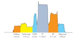
1. A plot of supply current vs. time during a wireless data transfer reveals distinct phases of operation.
When you’re considering how a battery-operated device will work, you need to understand the characteristics and constraints of the batteries themselves. Tradeoffs are typically made between cost, physical dimensions, capacity, and lifetime. Electrical discharge and recharge characteristics also play a key role in selection, as does tolerance to overstresses such as short-circuit behavior and extreme temperatures.
The familiar 1.5-V AA alkaline batteries have a capacity around 2700 milliamp-hours (mAh), for example. The smaller form-factor 3-V CR2032 lithium coin-cell batteries are typically rated around 225 mAh and have an additional limitation of about 20-mA maximum discharge. Both of these are common solutions due to their low cost and small form factor. The higher-capacity lithium-thionyl-chloride (LTC) batteries find applications in metering, where their longer life and low self-leakage offset their higher cost. They typically have a 3.6-V nominal output and are limited to low output current.
Different chemistries also have different voltage characteristics as the batteries discharge or recharge throughout their lifetimes. Integrated circuits for battery-operated IoT devices are typically designed with these characteristics in mind, providing low-voltage operation, failsafe circuits as batteries deplete, and overvoltage protection during charging or initial installation.
The operating life of the battery-operated IoT thing can be roughly estimated by the capacity of the battery pack divided by the average current drawn from the battery. IoT devices are designed to minimize this average current consumption, and how that’s done depends heavily on the application profile, meaning the proportion of time and energy spent in the each of its fundamental activities.
Energy Consumption Profile
The proportion of time spent in each activity phase strongly influences where battery-lifetime optimizations can be most effective. IoT sensors typically spend the vast majority of their time asleep, so idling the device for low sleep power is a must.
Semiconductor devices for IoT are designed for ultra-low leakage, a few microamps in a retained state, on par with the self-discharge rate of the battery. This residual leakage supports circuitry that remembers the state of the device (for example, its wireless connection information) for quick resumption of activity once awakened. It’s also important to understand how much additional power is required to exit the sleep mode and become fully operational again, since sleep mode gains can quickly evaporate with inefficiencies in required wakeup operations.
Energy consumption in sensing operations can vary widely with an application’s specific requirements, but often scale with the processor MIPS (millions of instructions per second) required for the task. Overhead energy consumption in the sensing phase occurs in resuming operation from sleep, in operating sensor circuitry, in executing microprocessor instructions, and then again in configuring the part to go back to sleep. Power efficiency for MCUs is typically expressed in datasheets in units of µA/MHz, at one or more clock rates. Efficiencies at lower clock rates are generally lower, due to static overhead current consumption.
The energy-consumption profile is also a strong function of the selected RF communications link, and choosing the most appropriate wireless protocol requires firm understanding of the system constraints. Beyond overall energy-consumption targets, you need to consider the required data rate, the RF transmission band, message delivery reliability and latency, wireless transmission range, tolerance to interferers, complexity of software, security, peak power limitations, and cost.
Wi-Fi can deliver up to 72 Mb/s over the air on a single 20-MHz channel, but its power consumption is too high for most battery-operated IoT applications. BLE offers 1 Mb/s over the air, effectively around 250 kb/s delivered, with good power efficiency, but its star topology can’t handle many nodes. ZigBee and Thread offer the resilience and scalability of mesh networking, but with effective data-transfer rates well below the 250 kb/s over-the-air bit rate.
2. The energy consumption for each phase is calculated as the area under the curve.
All of these technologies operate in the 2.4-GHz ISM band, which suffers from limited range. Going to RF bands in the range 168 MHz to 969 MHz, 802.15.4 standards offer many well-studied modulation schemes promising low power consumption and high link budget, typically with low data rates and customized software stacks. While these standardized protocols may provide ecosystem benefits and development partnership opportunities, many designers opt for fully custom wireless protocols to meet their specific targets.
Considering power constraints, frequent high-power RF transmissions may dominate energy consumption of the device, and they may violate battery peak-current constraints or necessitate a bulk capacitor to source peak current. Resorting to low-power narrowband transmissions may solve the peak power issue, but not the overall consumption because the transmitter needs to be on for a longer time. In the receive direction, long periods of time spent sniffing the RF band or resynchronizing to a network represent inefficiencies as well, which can affect system costs associated with both the price of crystal references and the energy they require to maintain coarse protocol synchronization through sleep intervals.
The point of identifying all of these interrelated constraints is that selecting the best protocol is certainly not a one-size-fits-all consideration. It can impact the cost of key items in the system, including the RF transceiver, the power management, timing references, and the MCU with its software, memory, and collection of peripherals.
Application Profile for an IoT Device
Let’s consider the example of a nifty IoT device: a wall-mounted, battery-operated Thread wireless dimmer switch featuring a touchpad to dim the lights or change their color. The lightbulb itself is connected to the power mains, but the wall switch is battery-operated. Thus, you can place it anywhere in the room easily, relocate it when you want to, or even place it in a mobile remote-control unit.
In a first implementation, which we’ll call the synchronous implementation, we have a device that spends most of its time asleep, waking up its MCU briefly eight times a second. Each time it wakes up, it operates capacitive sense circuitry designed to detect the presence and location of a finger on the touchpad. If no finger is detected, it goes right back to sleep. If a finger is detected, its positions on the touchpad over time are processed through a gesture-recognition algorithm in a microcontroller, so that a swipe-left dims the light, for example, while a swipe-right brightens it.
When a valid gesture is recognized, the device connects via Thread to an RF mesh network to send a control message to the light bulb. Upon acknowledgement from the router, the device again goes back to sleep until the next touchpad activation. The device is built using an EM3587 ZigBee/Thread system-on-chip (SoC) device and EFM8SB1 8-bit MCU (both supplied by Silicon Labs).
In our second implementation, which we’ll call the wake-on-touch implementation, the dimmer is built with an EFR32 Wireless Gecko SoC from Silicon Labs, configured to wake up on detection of a finger touch, rather than periodically. The finger-touch detection triggers further MCU-driven evaluation for finger gestures. Again, a valid gesture results in connection by Thread to the lightbulb, and then a return to sleep mode. While the first implementation is built and measured, the wake-on-touch implementation is a paper design.
Sleep
In both of these implementation options, planning for battery life involves considering sleep-mode energy consumption, device response time, and requirements of the RF communication link.
To minimize sleep-mode energy consumption in an IoT wireless MCU, most processes in the device are halted, and some circuits may be powered down. Circuits that typically need to remain active include power-management circuits that control the sleep and wakeup sequences, I/Os that retain the state of the device pins, oscillators and wakeup timers that provide timing references, and internal logic and memory retaining the state of the device for eventual wakeup and operation.
In our synchronous implementation, we chose a minimum leakage configuration, consuming about 1.5 µA, enabling a low-power RC oscillator and wakeup timer in the EM3587 to wake the MCU in the dimmer every 125 ms. The 125-ms number was chosen for latency below what would be noticeable to the user. Our wake-on-touch implementation enables additional asynchronous threshold detection circuitry during sleep mode, increasing the leakage to 6.7 µA, but optimizes response time to a finger touch and eliminates the need for periodic MCU wakeup to check the touchpad.
The sleep mode is also limited by the Thread protocol, which requires connection of the device to the mesh at least once every 320 seconds, by default. For safety margin, we configure the device to connect every two minutes. If the dimmer switch doesn’t check in on time, the mesh can report the device as being out-of-order, for example when the battery eventually dies.
Sensing
The dimmer switch uses a capacitive sensor, which includes an array of special-purpose output drivers and input amplifiers connected to rows and columns on the touchpad, detecting capacitance changes related to position of the finger on the touchpad. The analog information is captured by an ADC, filtered, and stored in a buffer. The buffer contents are processed by software to confirm presence of a finger on the touchpad and to recognize movements of finger position, known as gestures.
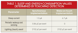
Touchpad detection determines the values for sleep and sensing energy consumption for the synchronous and wake-on-touch implementations.
Preparing the SoC for gesture recognition involves restoring operational power-supply levels to required circuits, turning on and settling oscillators for timing references, and restoring the logical context to the microprocessor digital core before proceeding with the execution of the algorithm in microcode. After sensing and possibly the RF connection are completed, the device goes back to sleep, reversing the power-up sequence of events.
In our synchronous implementation, a low-power wakeup timer fires periodically and triggers a series of microprocessor instructions to detect the presence of a finger. In our wake-on-touch implementation, the capacitance sensor operates autonomously, generating a trigger only upon detection of a threshold crossing due to a finger touch. This autonomous operation requires additional current, but means that the microprocessor needs to operate only when the keypad is actually touched, which may result in overall power savings.
Table 1 shows expected values for sleep and sensing energy consumption for the synchronous and wake-on-touch implementations. It reveals an increase in sleep current, a decrease in periodic wakeup current, and the same value for a touch event, since the gesture-recognition power consumption is dominated by the current required to drive the external capacitive touch network.
Connection
The dimmer switch connects with the wireless mesh network every two minutes and checks for messages from the internet gateway, in an operation called the long poll transaction. It also checks with the network for system updates every 30 minutes during the over-the-air query transaction.
In our dimmer switch, we use Thread mesh networking, which leverages the 802.15.4 DSSS-OQPSK physical layer in the 2.4-GHz ISM band. Thread enables IoT devices to be addressable using IPv6, allowing easy translation at a border router to internet traffic, and therefore access from virtually anywhere in the world. This means you could use an iPhone to remotely monitor or dim your light bulb, and you could read whether your battery-operated wall switch was online or it needed a replacement battery, or even the timestamp of the last time someone used it.
A significant part of an IoT device’s energy consumption may be spent on RF communication, so careful design of active power consumption is a must. Figure 1 shows the current-consumption profile of the EFR32 SoC captured during a data poll packet transaction.
The beginning of the waveform corresponds to the power-up and wakeup of the device and preparation of radio and packet information for transmission, labeled with identifiers 1-4 on the plot (Fig. 1, again). The CSMA portion of the waveform, labeled 5, occurs when the device is detecting whether there’s another transmitter on air before beginning transmission. The transmit portion, labeled 6, is the highest power-consumption phase. The peak sustained current is around 18.6 mA, with a short transient slightly above 20 mA, which is just within the tolerable limits of a single coin-cell battery. Packet transmission is followed by a receive mode awaiting acknowledgement. After receipt and processing of the acknowledgement, the device goes back to sleep.
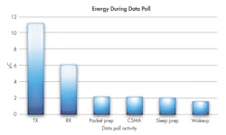
3. Analysis of the wireless transaction can identify candidates for optimization.
The entire transaction is seen to be 3.3 ms, and the integrated current over that interval is measured to be 26.5 µC (Fig. 2). Figure 3 plots the energy used in each phase of the wireless transaction and shows that the transmit (TX) portion dominates the power consumption. The same transaction using the EM3587 SoC consumes 55 µC.
Lifetime
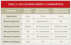
A convenient way to add up total energy consumption for each implementation is to calculate the charge consumption for each event (in µC) times the number of events per day (Table 2). For sleep and battery self-discharge current contributions, multiply the total leakage current (in µA) times the length of a day, in seconds. The sum of these µC/day charge consumption values translate directly into mAh per day battery consumption. Differences in power consumption in data poll and OTA query transactions between the two implementations are due to energy-efficiency improvements in the EFR32 SoC device.
Energy consumption can be calculated by multiplying the charge consumption for each event by the number of events per day.
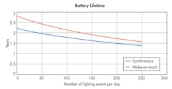
Figure 4 plots the expected lifetime of the dimmer battery for each implementation, as a function of the average daily activity at the touchpad, assuming a single CR2032 battery with 200-mAh usable capacity. With no touchpad activity whatsoever, we could expect a lifetime of around 2.4 years for the synchronous solution and around 2.9 years for the wake-on-touch version, driven by the average sleep-mode power consumption and self-discharge of the battery.
As activity increases to 200 touches per day, the lifetime diminishes to 1.5 years for the synchronous solution, corresponding to around 110,000 touchpad events. For wake-on-touch, this same condition results in about 1.75 years, or 128,000 touchpad events. Extending the curve to the right (Fig. 4, again) shows superiority of the wake-on-touch solution even past 500 touches per day.
4. The expected battery lifetime of a dimmer battery is a function of the average daily touchpad activity.
Total Energy Consumption
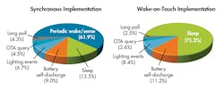
To optimize battery life, it is useful to compare energy consumption per day in each operating mode. Assuming 30 lighting events per day, the proportion of energy consumed in each of the states of the device is shown in the pie charts in Figure 5, along with the effects of battery self-discharge.
In the synchronous solution, the largest contributor by far is the periodic wake and sense operation at 61.9%, followed by sleep at 13.5%. Allowing greater latency in detection by increasing the interval between wake events would likely result in greatly improved lifetime. In the wake-on-touch implementation, 75.3% of the battery life is spent in sleep mode. Improvements in sleep-mode currents would be the most beneficial for battery lifetime.
5. Periodic wake/sense dominates synchronous implementations, while sleep mode dominates wake-on-touch implementations.
These results are not surprising, given the tradeoff of increased sleep-mode current consumption in the wake-on-touch solution. The periodic wake/sense and sleep figures together for the synchronous solution are 75.4%, nearly identical to the wake-on-touch sleep mode percentage.
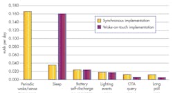
Beyond reviewing the proportions of energy spent in each mode in each implementation, it’s also helpful to compare absolute consumption. Figure 6 confirms that the primary improvement for wake-on-touch capabilities lies in the tradeoff between total periodic wake/sense and sleep energy, while incremental improvements are related to the power efficiencies of the wireless SoC’s RF transactions.
6. A chart of absolute energy consumption per day reveals tradeoffs in implementation.
Keys to successful design of a wireless IoT device include characterizing the device’s sleep, sense and connection intervals, and then further analyzing energy consumption within each task. Armed with an understanding of the tradeoffs of each contribution to energy efficiency, the IoT device developer can optimize a battery-operated wireless-node design for enhanced functionality and longer battery lifetime.
