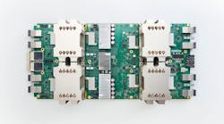
A year ago, Google revealed the custom chip that it built in secret to accelerate machine learning tasks in its data centers. On Wednesday, the company unveiled a second generation of the chip, which is capable of not only running software but also training it.
The next generation of the tensor processing unit – more commonly known as the TPU – is the latest sign that internet companies are growing impatient with slowing improvements in computer chips for machine learning, which involves training programs on reams of data and then applying the lessons to new information.
Google's first chip was only capable of make judgments with what it had already learned. But the newest TPU can also run the vastly complex algorithms used in training, a vital part of the process that involves leafing through hundreds of thousands of images or search terms, learning the difference between them without explicit programming.
The announcement suggests a shallow but deepening wrinkle in the semiconductor industry, which has struggled with the end of Moore’s Law and slowing improvements in computer hardware. Last year, Google said that its chips were around three processor generations (or around seven years) ahead of the next most advanced chips.
At the same time, chip suppliers are pouring billions of dollars to stay ahead of the machine learning demands of cloud companies like Google and Microsoft, which has also devised custom chips for data centers. Google’s latest chip is a potential threat to Nvidia, which claims that its graphics chips are significantly faster than TPUs at training and inferencing tasks.
Last week, Nvidia revealed that it had spent $3 billion on its latest accelerator chip, which contains specialized “tensor cores” to perform 120 trillion operations per second for deep learning. Inside the silicon slab are more than five thousand processor cores and 20 billion transistors to divide and conquer sophisticated software.
On the other hand, Google’s latest accelerators deliver up to 180 trillion operations per second – or 180 teraflops – on machine learning workloads. Jeff Dean, a senior fellow at Google, said in a blog post that the hardware – similar to Nvidia’s– contains a “custom high-speed network that allows us to build machine learning supercomputers we call TPU pods.”
The pods contain 64 second-generation chips, providing up to 11.5 petaflops of computation. Dean claims that only eight of the second-generation chips could train a Google translation program in an afternoon, where it had taken a full day for 32 graphics chips to train the same software. The company has said little else about the performance.
Nvidia did not respond to a request for comment.
Google is making the new accelerator available on its cloud, where it can be matched with other types of hardware, including Intel computers and Nvidia’s graphics chips. In addition, the company is offering free access to a cluster of a thousand cloud TPUs to researchers working on open machine learning projects.
These maneuvers could complicate Google’s relationship with Nvidia, which called out the cloud computing firm as a customer in its annual report. Last week, Nvidia launched its own cloud platform, where businesses could rent out its latest Tesla V100 chips, which is designed to be paired with computer chips from suppliers like Intel.
Updated May 14th, 2017: An update to this article added context about the competitive landscape for machine learning hardware. It also clarified how machine learning works as well as the back-and-forth announcements that seem to have Nvidia and Google on a collision course.

