Download this article in PDF format.
At first glance, using an external flash device with a microcontroller (MCU) appears to be a simple exercise in matching the two devices to achieve functionality. But designing an embedded product is a complex process of finding the best balance between competing solutions to meet the design requirements.
Introducing flash to the design, as most Internet of Things (IoT) devices do, adds another set of variables to arbitrate—and can make it more difficult to meet the application’s efficiency, longevity and reliability requirements. This article discusses the most common flash technologies incorporated in embedded systems and the challenges that emerge in order to reliably use them.
Types of Flash for Embedded Applications
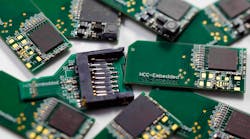
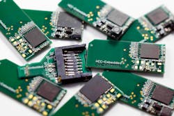
Flash can be either removable or non-removable. Removable media include USB pen-drives, compact flash, SD/SDHC/XDHX/MMC cards, and other similar packaged technologies. Non-removable media include NAND, NOR, and eMMC. Figure 1 shows eMMC-packaged NAND flash.
1. Packaged eMMC flash can be a fundamental building block in a reliable or deterministic storage system.
Removable Media
Practically all removable media is made from a packaged array of one or more NAND devices managed by an FTL embedded in an ASIC, FPGA or similar controller. Its main characteristics—high density, integrated flash translation layer (FTL), fast, and accessible--can be moved to a host system.
Engineers must take seriously the potential risks of using removable media in an embedded system. Most removable media are simply not capable of handling data storage reliably and they are typically not specified for use in embedded systems. The few that are tend to be more expensive. Even SD cards marked as ‘Industrial’ typically only have an enhanced operating temperature range. Removable media can be a benefit for consumer goods but more problematic for industrial applications like data loggers. Removable media is generally unreliable, can lead to uncertainty of data and suffers from unreliable contact and vibration issues.
Removable media can only be read by a compatible host system. This often forces the choice of file system to the eponymous file-allocation-table (FAT) system with all its known limitations. Most removable media have no chance to achieve fail-safety or establish controlled data commit points that can guarantee the state of a card. This is a real problem for reliable, fail-safe operation and presents a risk to data and to file-system integrity. Most SD cards are optimized for high speed at the expense of correctly defined behavior in the event of unexpected reset. Also, there’s no method for differentiating between critical and non-critical operations.
Non-Removable Media
NAND, NOR, and eMMC are amongst the most commonly used types of embedded flash memory. Compared with NOR, NAND flash presents some complex system-design issues.
NAND Flash
NAND flash is characterized by low cost per bit, combined with fast erase and write times. The address bus is multiplexed on to the data bus to reduce electronic complexity. It’s now the core storage technology used in a vast array of storage devices from SSDs to SD cards to eMMCs. When it comes to meeting high-density and performance requirements, NAND is the choice.
NAND flash is arranged as a set of blocks, each of which is divided into physical pages. Every page contains an area for data and a spare area that’s used for NAND management data. It’s increasingly common for NAND flash to consist of multiple planes that can be addressed independently and programmed or erased in parallel.
Three primary features of NAND flash contribute to the design challenge:
- An error correction code (ECC) is required to correct data that hasn’t been stored correctly.
- NAND flash is delivered with a small number of bad blocks, and during the life of the device, additional blocks may become bad.
- If the device will undergo heavy usage, a system of wear leveling is required to extend its lifetime.
Many other smaller features need to be considered on a device-specific basis. NAND flash technology is experiencing rapid and dramatic changes. Originally single-level-cell (SLC) flash was used, but has since progressed to multi-level cell (MLC) and now to triple-level cell (TLC) and 3D NAND. About 15 years ago, a single NAND device could store 32 MB—nowadays it can store 128 GB or more. (Moore’s law cannot keep up with NAND flash development!) This progression has led to higher densities and cheaper cost per bit, but has also changed the physical character of the flash.
SLC flash used to be able to survive 100K erase/write cycles with just 1-bit ECC correction, while the latest NAND can require 40-bit ECC correction per 528 bytes just to guarantee 3K erase/write cycles. Other technical challenges must be confronted, too, such as page-pairing issues and read disturb. Consequently, software to manage NAND flash has to progress with the new design features to meet reliability requirements.
If your design requires a NAND with more than 1-bit ECC correction, it will need to use a microcontroller with support for ECC calculations that match the NAND flash.
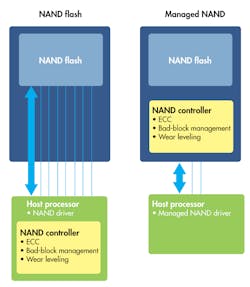
Serial NAND flash: One useful variant of NAND flash for embedded designs is serial NAND flash. It’s not available in the same huge densities as others, but carries two primary advantages: a simpler electronic interface using SPI, and (in most cases) the ECC calculation is integrated, making it possible to integrate with a wider range of MCUs. Figure 2 shows a traditional NAND flash controller built into an MCU.
2. When comparing raw NAND versus packaged NAND, several important should be considered, such as ECC requirements and the need for complex management services like wear leveling and bad-block management.
NAND Use Considerations
Wear leveling: Flash cells have a limited life and can only be erased and programmed a certain number of times before becoming unreliable—in effect, they wear out. Wear-leveling algorithms are used to increase the chip’s lifetime by moving the data between physical blocks to ensure some cells aren’t overused in comparison with others. These algorithms can be fine-tuned to match performance requirements.
ECC: The worst-case rate at which wear occurs is defined by the flash manufacturer. ECCs are used to ensure the data is always consistent if used within the chip specification. The strength (number of bits) of the required ECC is defined by the worst-case bit failure rate.
Bad-block management: Flash memory contains blocks that may be error-prone or unusable when the device is new. During operation, data in good blocks can later be corrupted by charge leakage or disturbance from writes in adjacent parts of the chip. Software is used to provide management of bad blocks and maps unusable areas to ensure that data are not corrupted.
Read disturb: Read disturb errors occur when a read operation on one page causes one or more bits to change in other pages of the same block. Executing many read operations on pages within a block, with no intervening erase of that block, increases the risk that bit errors will develop.
While NAND flash is the leading flash-storage technology used for large quantities of data, there are several important things to consider when using it. The error characteristics of each NAND device type are different, such as the number of bad blocks, bad block markers, and ECC requirements. This means ECC requirement has to be matched to the microcontroller’s NAND controller interface. NAND flash also needs complex management services such as wear leveling and bad-block management.
Flash Translation Layer (FTL) for NAND
Because of the requirement to re-map bad blocks, it’s not possible to treat a NAND device as a linear array of memory in most applications. In applications where flash is erased and rewritten many times, it’s necessary to introduce wear leveling to increase the life of the device. Both issues require a logical translation of the physical blocks.
These problems are resolved by using a software-based flash translation layer (FTL). From an application perspective, the FTL presents an array of logical sectors that hides the underlying complexity of the physical device, allowing a file system to use it like any other media driver.
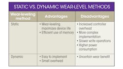
An FTL should also address the problem of wear leveling. There are two common approaches, static and dynamic wear leveling. In dynamic wear leveling, the system chooses the least-used block for the next write operation. This method is relatively weak, since it doesn’t account for data blocks whose contents remain unchanged.
With static wear leveling, under-used blocks are swapped in to distribute the wear across the whole device. Static wear leveling needs to be carefully tuned to ensure that block swapping doesn’t contribute unnecessarily to device wear. This is typically achieved using thresholds to determine sensible limits for swapping blocks. The table breaks down the static and dynamic wear-leveling methods.
NOR Flash
NOR flash, which pre-dates NAND, was used in a range of applications. NOR still has a very important share of the embedded-design market because of its relative simplicity and reliability. There’s no ECC requirement to guarantee 100K erase/write cycles, no bad blocks at manufacture, and a much simpler architecture. The price to pay for the increased reliability is much longer erase and write times, though. However, like all flash, using it in terms of being reliable is complex and requires a detailed understanding of the technology.
NOR flash comes in two main forms: parallel NOR flash, where the address and data buses are directly connected to the MCU; and serial NOR flash, which only uses an SPI interface (or similar) to communicate. Typically, serial NOR flash has densities <1 MB up to 128 MB. Parallel NOR flash can be much larger.
If NOR flash is to be heavily used, then it still requires a management layer (often an FTL) to provide wear leveling and ensure that the device is used evenly. Having such a layer will also manage any developed bad blocks.
NOR flash can be more expensive than alternatives, and it has relatively slower erase and write times. There’s no requirement for ECC, but to use it effectively, logical to physical mapping is required to be able to provide wear leveling,
eMMC
eMMC addresses many of these issues, thanks to several features. For instance, a simple block-mode interface hides all intricacies of the underlying flash from the user while the level of service is given by the manufacturer at the block level. Different write modes allow the user to optimize performance depending on whether the data being written is critical or not. Typically, file system meta-data is critical and file data isn’t so critical, but that also depends on the application and the level of fail-safety provided by the file system.
In addition, a bidirectional parameter exchange allows the card to optimize its operations based on the properties of the host system. Finally, eMMC reduces vibration and unplanned removal issues because it’s offered as a solid-state chip integrated on the target board.
eMMC devices can provide a fundamental building block in a reliable or deterministic storage system with clear advantages over other similar technologies. But as with any concept of determinism or reliability, the whole system has to be considered and the various components validated both individually and in the context of the complete system.
Challenge of File Systems When Using Flash
It can be a serious quality issue for an embedded system if the file system, or its contents, become corrupt. To establish tests and verification at the design and implementation stage, the designer must address fundamental challenges, including how to handle file operations and directory structures, how to deal with the integrity of data during power loss or unexpected reset, and how to verify correct operation of the flash.
Traditionally, the handling of file and directory operations is delegated to an embedded file system. An application gets significant benefits from using a file system—the abstraction of the storage media to a set of data files.
However, a file system alone can’t guarantee the integrity of data and the file system itself. Whatever method of ensuring fail-safety is used, the system remains dependent on the storage media and must define a required level of service from that media.
A system designed to ensure reliability must include a clear understanding of the critical exceptions—such as unexpected reset or power loss—and how each part of the system will meet the requirements of the components using it upon such an occurrence. Simply using a file system that claims fail-safe operation or journaling has no chance of guaranteeing reliable operation without defining these things.
Power Loss, Unexpected Reset, and System Failure
In an embedded application, if the data (or meta-data) managed by the file system becomes corrupt, the result could be catastrophic. For example, a file system stored on NAND flash may require reformatting, which will mean loss of all data. For this reason, it’s mandatory to use a fail-safe system in which the data is valuable, and furthermore, the application must be reliable.
A truly fail-safe file system will guarantee that all meta-data it manages on flash will always be consistent, and that any write to flash by an application (typically a file system) will be completed atomically. The atomicity of a write means that either the write operation is completed or the disk is left in the same state as it was prior to initiation of the write. This means the file system can guarantee the integrity of the data passed to it by the file system.
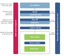
To ensure a fully fail-safe embedded system, each layer from the application level to the physical driver must specify what it requires from the adjacent layer. This is the only way to guarantee true fail-safety. For example, a generic FAT file system would require that multiple writes to different areas of the media be completed atomically. This is logically impossible to guarantee on a system where unexpected resets may occur. To build a reliable application, a fail-safe file system can be used together with another fail-safe file system.
3. Fail-safety system requirements: No file system can claim to provide fail-safety on its own—a system-wide design is required.
Required characteristics of fail-safe system (Fig. 3) include:
- After a system reset, the file system will always be in a consistent state.
- Any file that was opened for writing at the time of an unexpected reset will be returned to its pre-open state, unless a flush or close operation on that file was successfully completed. This means that the application developer is entirely in control of when the new state of a file is set, independent of any other activity in the file system.
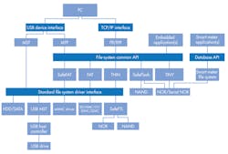
- Fail-safety of any file system (Fig. 4) can only be guaranteed if the low-level driver guarantees a defined quality of service (QoS).
For the file system, this is defined as:
- Any write operation must complete successfully or return an error. Otherwise, the file system must be restarted.
- All writes to the media must be executed in the sequence in which they’re provided to the driver.
- An erase operation must complete successfully or return an error. Otherwise, the file system must be restarted.
In practice, this means that the hardware has to provide some level of voltage protection. This will ensure that the system can take appropriate action if the voltage provided to the flash media is falling toward the specified programming voltage.
System Performance and Efficiency
To achieve high performance using a complex flash device such as multi-plane NAND or an array of NAND chips, it’s required that an FTL can read, write, and erase multiple devices in parallel. This could theoretically be achieved simplistically at a driver level. However, it would result in inefficient utilization of flash and, therefore, would be unlikely to be truly fail-safe. It’s better to address this problem at the FTL level, and it can be done with commercially available products.
4. HCC Embedded offers fail-safe file systems for all flash types. They include high-efficiency SafeFlash for products in which data integrity is critical, and full-featured TINY for resource-constrained applications, so that designers can choose the file system that best suits their needs.
When assessing performance, it’s common to measure the response by performing contiguous-read, contiguous-write, random-read, and random-write operations. In general, achieving high performance with contiguous read and random read is relatively straightforward. Contiguous-write and, more critically, random-write operations are more difficult to perform efficiently. This is the case for all flash-based memory devices. But by implementing sophisticated algorithms and system tuning, it’s possible to achieve significant improvements in performance.
Power-Management Considerations
Designers should use careful power management to ensure the flash device isn’t erased or written when power levels are outside of the manufacturer’s specified limits. If this isn’t the case, then problems may occur with the integrity of blocks and data. A well-designed FTL will specify the requirements of the low-level driver, including power requirements, to ensure fail-safe operation. Designers should request these specifications from the software supplier. For example, when the voltage supply falls to the specified minimum, then brownout detection should notify the system so that this condition can be managed.
At first glance, using an external flash device with an MCU appears to be a simple exercise in matching the two devices to achieve functionality. However, developing an application with efficiency, longevity, and reliability requires a comprehensive system-level approach. It’s hoped the issues highlighted can go some way toward helping designers address these fundamental technical issues.
References:
