Download this article in PDF format.
An embedded field-programmable gate array (FPGA) is an IP block that allows a complete FPGA to be incorporated in a system-on-chip (SoC) or any kind of integrated circuit. Embedded FPGAs are new, but the traditional idea of how chips turn into IP blocks has become old: RAM, SERDES, PLL, and processors are all routine IP blocks that used to be standalone chips. Now, FPGA is an IP block, too.
Users of embedded FPGA are NOT users of FPGA chips. Most FPGA chips are employed in lower-volume systems as “quick design, low NRE” ASICs. Embedded FPGAs typically target high-volume chip designs from major chip companies and large systems companies that have the volume to design their own ASICs.
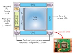
The diagram shows how an embedded FPGA core is just the programmable logic and interconnect—exactly like that of an FPGA chip, where the core is surrounded by various types of I/Os and PLLs.
There are several, and very different, ways to take advantage of embedded FPGA:
- Customization: Use embedded FPGA to provide dozens of SKUs instead of $1M mask spins.
- In-system programmability: Use embedded FPGA to allow a chip, and the system it resides in, to be reprogrammed to handle new standards that didn’t exist when the chip was designed.
- Extend battery life.
Customization (and more?)
At older process nodes, such as 90 nm, mask costs were low. Microcontrollers have limited GPIO, but a wide range of serial-interface I/O standards are requested by different customers. So at 90 nm, a microcontroller might have dozens of SKUs where the only variation is whether the interfaces are I2C or SPI or UART or some mix.
At 40 nm, where the leading-edge microcontrollers are about to be designed, mask costs typically run about $1M, so offering dozens of SKUs becomes extremely expensive. In addition, even small changes require substantial re-verification, qualification, and months of delay.
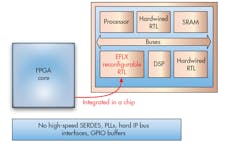
With embedded FPGAs, a small amount of reprogrammable logic on the peripheral bus can be used to program the serial-interface RTL. Therefore, any serial-interface protocol can be implemented on demand.
For example, in a Flex Logix EFLX-100 array, a UART takes 72 lookup tables (LUTs) and runs at 37 MHz (eHVT/SVT, 0.85V Vj, 125C Tj, Slow/Slow process corner). The amount of embedded logic can be sized as needed, depending on how many serial interfaces are desired in the target microcontroller. Microcontroller companies have their own register-transfer language (RTL), but also RTL that exists today for FPGAs from multiple vendors can be used in embedded FPGA. Notice that in this application, the customer doesn’t even know that embedded FPGA is in the microcontroller.
So now a single microcontroller die can be designed and then be made to look like dozens of SKUs. Thus, if a new customer comes along with a new combination, it can be offered quickly and cheaply. Plus, the inventory carrying cost goes down.
But wait, there’s more. In a microcontroller today, all of the I/O is processed by the processor. With embedded FPGA, it’s possible to implement state machines in the embedded FPGA to do local processing of the inputs and trigger outputs – which could both offload the processor and speed responsiveness.
Customization is also applicable to accelerators since numerous types of encryption are required by different customers who need multiple skews as well. Instead, an embedded FPGA on the processor bus can be programmed to offer whatever kind of encryption desired by each customer.
The benefit of all this to the chip company is that every SKU can come to market more quickly and from one design, thus increasing return on investment (ROI). Your CFO will be happy.
In-System Programmability to Keep Up with Changing Standards/Specs
Both the cost to design a chip and the time to design a chip keep increasing with each new process generation. Mask costs alone are $5M at 16 nm. Another major problem is that standards keep changing. A chip that can’t run the latest version of certain protocols is a chip that will have a short life, even if it cost a lot to develop.
Customers are also starting to demand in-system programmable chips. For example, in the data center, customers are envisioning a reconfigurable cloud (see the recent talk by Doug Burger of Microsoft) where all network, storage, and security protocols are programmable, not fixed as they are today. This will enable the data center to use chips and systems longer and keep performance high, while also allowing data centers to innovate within their own company.
The kind of programmability required isn’t possible with a processor core. For example, in a network interface or switch chip, the programmable logic needs to run up to 1 GHz operating on very wide data or control buses. The benefit to a chip company is that the chip can have a longer effective life. The benefit to a systems company is that its system and data center can have a longer effective life. Everyone gets a higher ROI and, once again, your CFO and your customer’s CFO will both be happy.
Extend Battery Life
Battery life in MCU and IoT applications is critical. Most battery usage is connected to the frequent, repetitive, low-level tasks, not the infrequent more complex operations.
Flex Logix recently did a detailed analysis for several low-level DSP functions that showed how a small block of embedded FPGA (TSMC 40ULP) could process the functions as fast or faster than the ARM processor, but using 2X to 5X less energy. The embedded FPGA offloads the repetitive, low-level tasks at lower energy and the ARM processor is only awoken when it’s time for a more complex task.
The initial perception of most customers is that an FPGA is power-hungry, but that’s because most FGPA chips on the market are optimized for leading-edge processes and leading-edge performance. Flex Logix’s TSMC 40ULP implementation has been optimized for low power for a variety of tasks, including 0.5-V state retention and even the option of operation at 0.5 V if desired.


