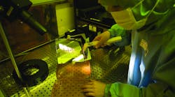
Year after year, semiconductor equipment maker ASML has been saying that the industry's golden goose is about to hatch. After more than two decades, it still hasn't.
ASML's extreme ultraviolet lithography systems have been too slow and expensive for customers like Intel and Samsung. But the technology – more commonly known as EUV – has survived because it can etch far smaller circuits onto silicon chips than today's machines, which still mint postage stamps of silicon with billions of transistors.
Now, ASML's customers are lining up for machines. The company revealed last week that it had received eight orders for EUV systems in the second quarter this year. That gives it 27 total backorders worth around $3.25 billion for the new silicon printing presses, which can etch circuits almost as small as single atoms using intense beams of light.
Using a 13.5nm light source, EUV machines trace microscopic patterns ono the surface of silicon wafers without having to expose the chips multiple times, an expensive manufacturing trick used by today's lithography tools to squeeze billions of extremely small circuits onto chips. The difference is that today’s equipment uses a 193nm light source.
Last week, ASML also released its second quarter business results, which are closely watched in the semiconductor industry for EUV updates. Based in Veldhoven, the Netherlands, the company reaped $2.45 billion in revenue last quarter and made two EUV lithography sales that totaled around $255 million.
The company also announced a breakthrough on the road to commercial EUV lithography, revealing that a laboratory system could spit out 125 wafers per hour. Technically, the system can produce that many wafers but has not been deployed in actual fabs. For years, companies have said that EUV would only make economic sense at that rate.
To do that, ASML has been trying to increase the brightness of the light source used in EUV equipment to 250 watts. The light source shines brighter at higher wattages, allowing the systems to pattern wafers in less time. For years, it has been considered one of EUV's biggest obstacles.
In 2013, the company acquired Cymer, the largest supplier of deep ultraviolet light sources used in semiconductor manufacturing, to help. But progress had been slow: The same year, Cymer announced that it had only pushed the brightness of an EUV light source to 55W.
But at the Semicon West trade show in San Francisco last month, the company said that it had finally reached 250W, according to industry trade publication EETimes. Over the years, ASML has shipped EUV systems to customers like Intel and semiconductor research centers like Belgium’s Imec, which have been testing the machines at lower power in actual fabs.
ASML, the world’s largest supplier of photolithography tools, said it will continue improving the productivity of EUV machines, which can cost around $100 million but only produce wafers around 70% to 80% of the time each day. In contrast, current lithography machines can stay on almost 23 hours per day.
The advances come as major chip suppliers pencil EUV into their roadmaps. Within the next two years, both Intel and Samsung want to start manufacturing 7-nanometer chips with EUV systems. TSMC, the chip industry’s largest contract manufacturer, has planned to build 5-nanometer chips using the technology in 2019.
ASML has also been riding the growing market for semiconductors, which technology research firm Gartner predicts will reach $400 billion this year thanks to soaring demand for memory chips. Its second quarter revenue grew more than 20% over the same time last year, up from around $2.03 billion.
Accordingly, ASML's recent uptick came from sales to memory chip makers, which are buying equipment to increase their DRAM and NAND wafer capacity. The company, which also does maintenance for customers, predicts that it will generate around $2.56 billion in third quarter revenue and sell three NXE:3400B systems, its latest using EUV lithography.

