Qualcomm is well-known for its 64-bit ARM-based solutions in the smartphone market, but its new 48-core Centriq 2400 processor targets the server space. The fully ARMv8-compliant processor is based around Qualcomm’s Falkor CPU. The chip uses 10-nm technology and incorporates the latest EL3 TrustZone and EL2 hypervisor support from ARM.
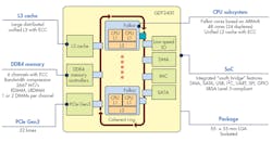
Each CPU core is paired with another core and a shared L2 cache into a duplex building block that’s linked to other blocks using a bidirectional segmented ring bus (Fig. 1). The system has an aggregate bandwidth of 250 Gb/s. The ring provides a fully coherent memory system as well as IO coherency support.
1. Qualcomm’s Centriq 2400 is built around pairs of ARMv8 Falkor CPU cores linked by a bidirectional segmented ring.
The chip has 32 PCI Express Gen 3 lanes and six DDR4 memory channels with ECC support. It supports 2667-Mtransaction/s RDIMM and LRDIMM memory with up to two DIMMs per channel. The memory controllers support in-line compression that’s transparent to the software, effectively doubling the memory bandwidth. The system also has SATA, USB SPI, UART, and I2C interfaces.
In addition, the system supports secure boot using an on-chip boot ROM, as well as OEM keys. Firmware performs anti-rollback checks.
The L2 cache is an 8-way, 128-byte/line interface with SEC-DEC ECC protection. There’s a 15-cycle minimum latency for an L2 hit. The cache system includes quality-of-service (QoS) support to improve cache utilization, thereby reducing data latency. A per-resource monitoring system and way-based allocation can be managed by VM, container, or thread group level.
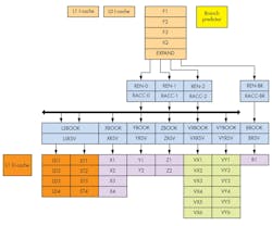
The Falkor CPU pipeline (Fig. 2) has variable-length pipelines tuned for each function, such as load/store (LDx/STx). It can issue four instructions per cycle, including one branch instruction and three non-branch instructions with single-cycle access to the L0 instruction cache. The L0 and L1 caches total 88 kB.
2. Variable-length pipelines in the Falkor CPU pipeline are tuned for each function, such as load/store (LDx/STx).
The branch predictor subsystem often imparts no overhead, or at most, an additional cycle if the predicted branch is taken. The 16-entry branch target instruction cache (BTIC) has no branch overhead. The system also features a multi-level branch target address cache (BTAC) for indirect branches and a multi-level branch history table (BHT).
Out-of-order dispatch support has a 76-instruction dispatch window. This is more effective in servers versus embedded systems, where the latter has to contend with interrupts and task switching.
The Centriq 2400 fits into a 55- × 55-mm LGA socket. The chip is Server Base System Architecture (SBSA) compliant, which is an open-source standard for 64-bit ARM processors that allow operating systems to work across platforms without modification.
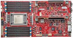
The system can be found in Microsoft’s Project Olympus platform (Fig. 3) designed for the Open Compute Project (OCP). All of Facebook’s data centers use OCP hardware.
3. The Centriq 2400 is being used in Microsoft’s Project Olympus Open Compute Project (OCP) platform.
Qualcomm isn’t the only player in this space. Cavium’s 64-bit ThunderX2 is available with 54 ARMv8-A Cortex cores. It also has a multi-issue, out-of-order (OOO) architecture, although it tends to target networking applications with its 100-GbE support.
Applied Micro/Macom’s X-Gene 3 is aimed at big data and cloud storage. Its SoC includes four 10-Gb/s Ethernet ports to support the 32 ARMv8-A cores. In addition, there are 32 PCI Express Gen 3 ports in addition to SATA controllers. The chip can handle up to 1 TB of DRAM.
The availability of Microsoft Server in this space could change enterprise views of the ARMv8-A platforms. This space has been dominated by Intel and AMD x86 platforms, with Linux and Microsoft Server hosted on most systems.


