New non-volatile memory technologies have significant challenges because flash memory is so well established. That’s not stopping the competition, though, and one of these may eventually replace flash memory as we know it. Crossbar’s ReRAM (resistive RAM) is one of those technologies.
I talked with Sylvain Dubois, Vice President of Strategic Marketing & Business Development, to find out more about ReRAM and how it compares to other technologies like Intel’s Optane.
Wong: How does ReRAM work?
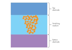
Dubois: The fundamental physics behind ReRAM cells (Fig. 1) are incredibly simple, making it easy to stack cells in 3D and scale to very small process nodes. The cells typically employ a switching material with different resistance characteristics sandwiched by two metallic electrodes. The resistance switching mechanism is based on the formation of a nanofilament in silicon-based switching material. Designers have substantial flexibility to optimize performance depending on the switching materials and memory-cell organization.
1. The resistance switching mechanism of Crossbar's technology is based on the formation of a filament in the silicon-based switching material when a voltage is applied between the two electrodes.
Regardless of the material specifics, developers of ReRAM technology all face several common challenges: overcoming temperature sensitivity, integrating with standard CMOS technology and manufacturing processes, and limiting the effects of sneak path currents, which would otherwise disrupt the stability of the data contained in each memory cell.
Crossbar ReRAM technology is based on a simple two-terminal device structure using CMOS-friendly materials and standard CMOS manufacturing processes. When an electric field is applied across the cell, a metallic filament forms across the cell and changes its resistive characteristics. Because the switching mechanism is based on an electric field, the cell behavior is very stable across a wide temperature range.
It can be easily integrated with CMOS logic circuitry and manufactured using existing CMOS fabs without the need for any special equipment or materials. As it is a low-temperature back-end-of-line (BEOL) process integration, multiple layers of Crossbar ReRAM arrays can be integrated on top of CMOS logic wafers to build SoCs, MCUs, and FPGAs with large amounts of 3D monolithic embedded ReRAM storage.
Wong: One of the greatest challenges facing developers in achieving ultra-high-density ReRAM (>1 Tb) has been overcoming the leakage (sneak) current problem in crossbar arrays that interferes with the reliable reading of data from individual memory cells. How do you address this?
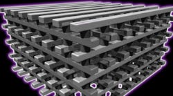
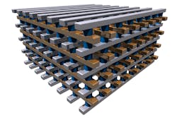
Dubois: Crossbar’s patented built-in selector overcomes the sneak current issue in a uniquely elegant way that enables Crossbar cells to be stacked, and employs a single transistor to drive as many as 2000 resistive memory cells with very low energy. It exhibits a broad range of device characteristics, providing high-density 3D arrays without occupying additional silicon area. These extremely dense memory arrays (Fig. 2), with the capability to scale below 10 nm, store multiple bits per cell, and stack 3D layers, provides a path toward terabytes on a single die.
Crossbar’s patented field-assisted superlinear threshold selector device is capable of suppressing the leakage current below 0.1 nA, and has been successfully demonstrated in a 4-Mb integrated 3D stackable passive Crossbar array. The high selectivity of the FAST device and its ability to be integrated directly into each ReRAM memory cell make it possible to move beyond the density limitations of 1T1R array structures and implement commercial memory products based on 3D stackable 1TnR memory architectures for ultra-high-density nonvolatile memory application. The typical primary benefits of higher levels of integration are higher performance, lower energy consumption, and lower cost.
Wong: Considering process manufacturing as well as cost, can you talk about the advantages of ReRAM compared with traditional flash-memory technologies, such as NAND?
Dubois: Crossbar ReRAM is a very scalable, high-performance, and low-energy technology that can be manufactured by any semiconductor foundry, such as CMOS logic fabs or memory fabs, using CMOS-friendly materials and process steps. The filament is ~4 nm wide, so this technology will scale below 10 nm.
Crossbar ReRAM is a BEOL technology, and the process steps required to manufacture the memory cell can be repeated to build very dense 3D ReRAM crosspoint arrays. Crossbar ReRAM has 100X lower read latency and 1000X faster write performance than flash. It has the capability to be 2X denser than 3D NAND, while most of Crossbar’s customers are looking for a performance boost by leveraging the low latencies of ReRAM.
Wong: When can we expect to see ReRAM in commercial deployments, and for which type of applications?
Dubois: Crossbar is now ramping up production with SMIC at 40 nm, and we have agreements in place to license our technology to a dozen of MCU/SoC companies. Our current developments are targeting embedded ReRAM IPs integrated in MCUs/SoCs for IoT, consumer electronics, artificial intelligence, and industrial applications. We are also working on 28 nm and more advanced process nodes with custom development programs.
Crossbar ReRAM will be ported to smaller process nodes to enter the data-center market as a storage-class memory layer (SCM). Crossbar ReRAM will expand its market share gradually toward higher-capacity storage solutions, while NAND will slow down its scalability path.
2. High-density ReRAM 3D array.
Wong: How do you compare with Intel 3D Xpoint and the fact that Samsung and Toshiba are putting 3D NAND into volume production?
Dubois: There is a huge market for lower-latency storage solutions, and we believe that ReRAM is a more scalable and manufacturable technology than PCM-based 3D Xpoint with lower-latency, lower-energy capabilities. In terms of business development, there are always benefits to see different players working on creating a new market segment and convincing data-center or mobile-computing architects to rethink system architectures to efficiently integrate these new added-value, storage-class memory solutions.
Wong: How does ReRAM compare to MRAM and PCM?
Dubois: Crossbar ReRAM is not addressing the same market applications as magnetoresistive RAM (MRAM) or phase-change memory (PCM). MRAM is targeting low-density SRAM replacement, as manufacturing complexity and scalability challenges will limit the use of MRAM for cost-efficient high densities.
PCM suffers from scalability challenges as well as it requires high current to generate the heat to change the material phase from poly to amorphous and vice versa. PCM won’t be able to scale to small process nodes due to crosstalk between the cells. Crossbar ReRAM does not suffer from crosstalk and is highly scalable. Our storage mechanism depends on an electric field, and we do not involve any phase change of the material.
Wong: How can ReRAM be used for applications such as IoT, deep learning, and AI?
Dubois: Having ReRAM and CMOS logic on same process node is enabling new memory-centric architectures that will revolutionize computing for deep-learning neural networks and artificial intelligence.
For technologies to produce rich sets of data that can be analyzed and acted upon, innovative memory technologies are needed to deliver high performance and low energy.
Non-volatile memory technologies such as Crossbar ReRAM are helping to address the performance and energy challenges of embedded IoT by delivering lower energy and lower voltage operation, monolithic integration with computing cores, and faster read and byte-addressable writes.
Crossbar ReRAM is a programmable non-volatile resistance that can be integrated with various logic gates to achieve new computational units. It can be easily integrated with standard CMOS logic processing, analog, and RF onto a single chip, enabling IoT devices with advanced computational capabilities while running at ultra-low energy, which is required for years of operation without a battery charge.
Sylvain Dubois joined the Crossbar Inc. management team in 2013 as Vice President of Business Development and Strategic Marketing. With over 17 years of semiconductor experience in business development and strategic product marketing, he brings a proven ability to analyze market trends; identify new, profitable business opportunities; and create precise product positioning that’s in sync with market demands to drive market-share leadership and business results.
Prior to joining Crossbar, Mr. Dubois led strategic product positioning and market engagement for developing new products at Spansion. Responsible for identifying new growth opportunities and expanding the product portfolio, Mr. Dubois was instrumental in defining the Spansion flash-memory product roadmap.
From 2002-2006, Mr. Dubois was a system-on-chip architect of OMAP application processors at Texas Instruments. Mr. Dubois was in charge of the architecture and technology roadmap of DRAM and flash-memory controllers, and developed strategic relationships with major DRAM and flash-memory suppliers.


