Download this article in PDF format.
RS-232 was the PC serial communications standard for many years. Hardware and software support for this simple, yet effective, interface was included on every PC made until it was eventually replaced by the faster and more complicated Universal Serial Bus (USB) standard.
However, RS-232 remains popular to this day for many serial-communications applications because of its simplicity and lack of required license fees. Software support for RS-232 is still supplied in the operating system of today’s PCs, and hardware support is available by adding one of the USB-to-serial adapters available from many suppliers.
One limitation of RS-232 is the relatively short distance required between connected equipment. The RS-485 standard solves this problem by replacing the RS-232 inputs and outputs with a differential driver/receiver. With few exceptions, RS-485 transceivers include a direction control to switch the driver between transmit and receive, thereby making the serial interface half-duplex only (one direction at a time). This is not an issue for equipment designed to handle the rapid direction change.
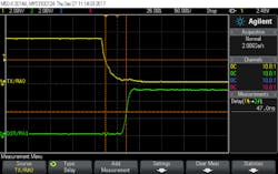
1. Programmable combinational logic senses the PC TX transmit start bit and switches the RS-485 direction to transmit in less than 50 ns.
But if you want to add the RS-485 hardware interface to your RS-232 serial output, you’ll need to implement an automatic direction control to manage the direction change in the data flow. Unfortunately, there aren’t any handshaking signals in the PC’s RS-232 interface fast enough to change the direction back-and-forth at rates required by serial communications.
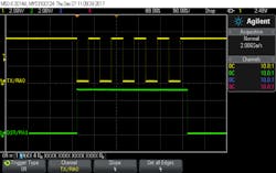
2. The start bit starts an internal timer to hold the direction control in transmit until the middle of the stop bit.
A microcontroller (MCU) such as the PIC10F320 has Core Independent Peripherals (CIPs) that are suited to easily solve this problem. CIPs reduce the need for external components, which in turn helps lower cost. Programmable combinational logic in the PIC10F320 can be used to sense the PC TX transmit start bit. Once detected, it’s able to switch the RS-485 direction to transmit in less than 50 ns (Fig. 1), and starts an internal timer to hold the direction control in transmit until the middle of the stop bit (Fig. 2). Pull-up and pull-down resistors on the RS-485 lines are used to maintain the RS-485 transmission line in the idle state for the duration of the stop time and any idle time that may follow.
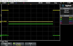
3. The microcontroller senses when the transmit stop bit is not present to extend the transmit direction control for signals.
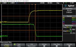
The microcontroller can also be programmed to sense when the transmit stop bit isn’t present to extend the transmit direction control for signals such as a BREAK (Fig. 3). The internal combinational logic holds the direction control in transmit until the PC releases the TX line. When the TX line goes high, the combinational logic switches from transmit to receive in less than 50 ns (Fig. 4).
4. When the TX line goes high, the combinational logic switches from transmit to receive in less than 30 ns.
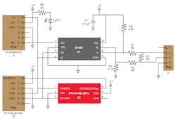
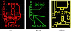
A typical hardware configuration is shown in Figures 5 and 6. Note that the transmit and receive direction controls are separate and the receive enable (/RE) is tied low. With the receiver always enabled, all transmitted data will be received. RS-485 bus collisions can thereby be easily detected by confirming that every character received matches what was sent.
5. Circuit diagram of RS-485 transceiver with automatic direction control.
6. Printed-circuit layout of RS-485 transceiver with automatic direction control.
The PC side of the configuration is shown as the connections to an ADM00393 USB-to-serial adapter. This adapter provides the software interface to the PC serial API functions and hardware interface at normal 3.3- or 5-V logic levels needed for the RS-485 transceiver.
The J3 programmer interface is shown as a convenient way to program the SOT23-6 device in-circuit. There is no need to populate J3 with a connector. A mechanical connection by inserting pins on the programmer, such as a PICkit 3, should suffice.
Code Development
The MPLAB X Integrated Design Environment (IDE), together with the XC8 compiler and MPLAB Code Configurator (MCC) plug-in, is an example of a way to simplify the code development process for this application. All can be downloaded (free) from Microchip’s website.
Open MPLAB X and use the File>New Project setup wizard to create a PIC10F320 project using C as the programming language. If you haven’t already done so, download the MCC plugin with Tools>Plugins Download. Enable MCC with the Tools>Embedded menu option or click the MCC icon in the toolbar. In the Device Resources window, add NCO1 and CLC1 to the Project Resources by double-clicking on them.
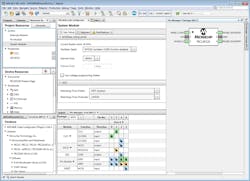
7. MCC system configuration selections for package, pins, oscillator, and watchdog timer.
The project window should resemble what’s shown in Figure 7 when you select the System Module in the System Resources window and the SOT6 package in the Pin Manager tab. Make the Internal Oscillator and WDT selections as shown.
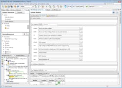
Click on the Registers tab to reveal and select the configuration word selections as shown in Figure 8.
8. MCC system configuration word selections.
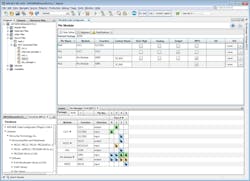
Select the Pin Module system resource and configure the pins as shown in Figure 9. Note that unused PORT pins A2 and A3 are configured as inputs with weak pull-ups enabled so that they’re not left floating.
9. Pin module configuration selections.
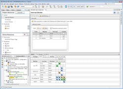
Select the Interrupt Module system resource and configure as shown in Figure 10.
10. Interrupt configuration selections.
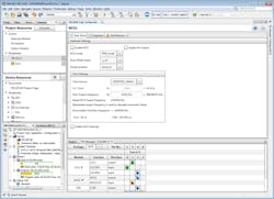
Select the NCO1 system resource and configure it as shown in Figure 11. The NCO1 Output Frequency is determined by dividing the desired RS-485 baud rate by 9.5. That will make one period of the NCO1 9.5 bit times. The example shows the NCO1 Output Frequency for a 38,400 baud rate.
11. Numerically controlled oscillator configuration selections.
The NCO1, which isn’t enabled initially, is started from 0 by the CLC1 interrupt and will set the NCO1 interrupt flag at the end of the first period. The interrupt is polled, so the NCO1 interrupts aren’t enabled. This is covered in more detail later.
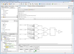
Select the CLC1 system resource and configure it as shown in Figure 12. The set-reset (S-R) latch is set by a falling TX start bit present on the CLCIN1 pin. The S-R latch is reset at the end of the first NCO1 period if the STOP bit on CLCIN1 input is high (CLCIN1 AND NCO1OUT). If it’s not, then software will reconfigure the CLC1 to reset the S-R latch on the rising TX signal by enabling the CLCIN1 true input to the Gate4 OR gate. The Gate4 OR gate output is inverted to ensure that the S-R latch remains reset during initialization. This will be removed as the final step of system initialization just before the main loop.
12. Configurable-logic-cell configuration settings.
The final step of the code configurator is to generate the code by clicking the Generate button in the Project Resources window. When the automated code is complete, all that remains to be done is a slight adjustment to the CLC1 initialization, the interrupt service routine, and the main routine.
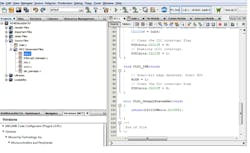
We need to add one line to the CLC1 interrupt service routine located in the clc1.c file created by MCC. This line, shown in Figure 13, enables NCO1.
13. CLC1 interrupt service routine code additions.
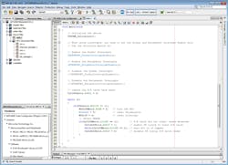
Finally, the interrupts must be enabled in the main routine, the CLC1 S-R latch reset removed, and main loop code added, as shown in Figure 14.
14. Code additions to the initialization and main loop.
The CLC1 interrupt starts NCO1. At the end of the first NCO1 period, the NCO1IF flag will be set. The main loop polls for this event and stops the NCO1 when it occurs. The NCO1 accumulator and interrupt are then cleared in preparation for the next start bit event.
The final step is to determine if the STOP bit was valid. If it wasn’t, the S-R latch will not be reset, and the CLC1 output will remain high. If this occurs, then the CLC is reconfigured to clear the S-R latch when the TX line (CLCIN1) goes high. Software then waits for this event indefinitely. When it finally occurs, the reconfiguration is removed, and the main loop goes back to waiting for the NCO1 interrupt.
Conclusion
If you would like to add the RS-485 hardware interface to your PC’s RS-232 serial port, you can add automatic direction control using a MCU with CIPs. This article demonstrated a typical hardware configuration for creating automatic direction control using a single 6-pin MCU and covered how to simplify developing code for this application. Although other solutions exist, this method offers the advantages of fewer components, lower cost, and better performance.
Ward Brown is a Staff Applications Engineer with Microchip Technology Inc.’s MCU8 Business Unit.

