Most FPGA vendors tend to focus on data-center workload applications, but a large percentage of users require different architectures for mainstream applications. Vertical markets needing mid-range FPGAs include networking, cellular infrastructure, defense, commercial aviation, industry 4.0, and other traditional FPGA applications. Such applications are driving a new set of dynamics.
System designers must achieve a combination of low power and cost without forfeiting performance and security. This means looking at FPGAs differently, using new process technology choices, device architectures, transceiver strategies, and built-in security measures. Also important is a new fabric design that’s able to meet mainstream performance requirements while minimizing power and cost.
Optimizing FPGA Fabric for Performance, Power, and Cost
To meet mid-range system requirements, an alternative class of FPGAs is being manufactured on silicon-oxide-nitride-silicon (SONOS) non-volatile (NV) technology on a 28-nm node. These FPGAs typically consume one-tenth the static power of alternative SRAM FPGAs, and half the total power. Some attributes of these FPGAs (such as the non-volatile configuration memory) directly reduce static power, while total power reduction indirectly affects reduction of die area in other cases.
These FPGAs also use a traditional fabric, one of the key features of which is LUT-4 for the logic element. Six-input LUTs can provide speed benefits, which is important for data-center acceleration, but four-input LUTs are the better choice for a power- and cost-sensitive mainstream markets. It’s been well-established that four-input LUTs can make more efficient use of a die area than six-input LUTs. A given user design can be implemented with less silicon area using a 4-LUT architecture than using a 6-LUT architecture.
One contributing factor is that a six-input LUT requires 4X more configuration memory bits (64 versus 16), but can only accommodate about 1.6X as much logic as a four-input LUT. This traditional observation applies even more strongly to advanced fabrication technologies because SRAM configuration memory hasn’t scaled as fast as ordinary logic, due to the need to mitigate the risk of single-event upsets (SEUs). In contrast, FPGAs that use a SONOS configuration cell are immune to SEUs.
Consider an FPGA cluster of 12 four-input LUTs versus a cluster of 8 six-input LUTs. The total logic capability of the cluster (i.e., the amount of user logic that the cluster can accommodate) is similar in each case. The larger fan-in of the six-input LUT means fewer levels of logic may be traversed by the critical path within each cluster, potentially reducing the total contribution of intra-cluster delay to the critical path. However, from the outside, the two clusters appear similar; they have a similar typical number of incoming and outgoing signals, and so the total length and delay contributed by the inter-cluster wiring is similar in both cases.
Figures 1 and 2 show clusters with different LUTs, but similar numbers of incoming and outgoing signals.
1. This cluster of three four-input LUTs has eight inputs and two outputs.
2. This cluster of two six-input LUTs also has eight inputs and two outputs.
Overcoming Wiring Delay, Clock Power Consumption
As process technology has progressed from 65 nm to 28 nm and beyond, the delay of wiring has come to dominate logic delay, due to poor scaling of metal wire and via resistance. To some extent, this can be mitigated by widening the wires, but that adds to the die area and cost. So, with each succeeding generation of process technology, inter-cluster delay becomes a significant contributor to the critical path, thus diminishing the speed advantage of six-input LUTs.
An example of the advantages of such a fabric design is Microsemi’s PolarFire FPGA family, which provides rapid direct connections between nearby LUTs. This can reduce intra-cluster delay, especially in conjunction with advanced synthesis and placement algorithms. Certain logic functions (such as MUX trees) greatly benefit from the direct connections.
Another focus of today’s latest FPGA fabrics is clock dynamic power. Clocks can be a significant contributor to dynamic power in mid-range system applications, often consuming nearly as much power as the rest of the routing and logic. For this reason, clocks should be designed to conserve power. This means allocating more area to clock wires to space them further apart, significantly reducing their capacitance and dynamic power.
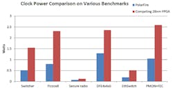
3. These benchmark results highlight clock power differences between FPGA implementations.
Flip-flops also must be designed to minimize clock power. To do this, clock gating is provided at two levels in the clock tree, as well as for each individual flip-flop, to avoid wasting power on unused branches. This can reduce clock power to less than half that of alternative 28-nm FPGAs, averaged over a suite of designs (as shown in Figure 3, which uses the PolarFire FPGA as an example of the new fabric approach).
The choice of operating voltage is also important. A power-performance tradeoff must be carefully optimized for a 1.0-V core logic supply. In the case of FPGAs fabricated with SONOS NV technology on a 28-nm node, this is somewhat less than the 1.05-V nominal voltage for the process on which it’s manufactured. Customers desiring extra speed still have the option to use the full 1.05 V supply.
New Math Path
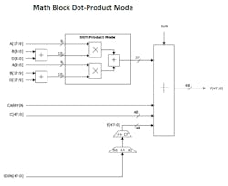
Finally, today’s latest FPGA fabrics take a different approach in the math block, ensuring it can support 18-bit multiply-accumulate operations (Fig. 4).
4. This is a simplified diagram of a math block’s dot-product mode logic.
Key new features as compared to earlier FPGA generations include:
- Provision of a pre-adder with a full 19-bit result. This eliminates the need for fabric adders when implementing symmetric finite-impulse-response (FIR) filters, saving power.
- Provision of an input value cascade chain. This reduces the need for fabric registers when implementing systolic FIR filters, again saving power.
- Accumulator widened to 48 bits.
In addition to the 18- × 18-bit multiplication mode, the math block should support reduced precision 9-bit operations. This includes supporting two independent 9 × 9 multiplies with no requirement for a common factor. Unlike alternative math blocks that can exchange two 18 × 18 multipliers for three 9 × 9 multipliers, this approach enables an FPGA to exchange one 18 × 18 multiplier for two 9 × 9 multipliers—a 33% improvement.
Even better, if the math block also supports a 9 × 9 dot-product mode (Fig. 4, again), the FPGA will provide an ideal solution for image-processing and convolutional-neural-network (CNN) applications. Compared to independent 9 × 9 multipliers, the dot-product operation reduces power in the following ways:
- No need for a separate fabric adder to sum the two products.
- The pre-adder is fully supported, allowing efficient implementation of symmetric 9-bit FIR filters or 2D convolution.
- All four factors are independent—designers of CNNs don’t rely on complex weight-sharing or input-sharing schemes to maximize resource and power efficiency.
New demands on FPGAs in a growing variety of mainstream, mid-range systems applications have led to fundamental changes in their design. This includes the use of new process technologies and architectures and new types of transceivers, as well as significant improvements to the basic programmable fabric logic. Fabric changes ranging from the LUT size and configuration to the design of the math block enable today’s FPGAs to meet the performance requirements of a growing range of mainstream systems while minimizing their power and cost.
Ted Marena is Director of Business Development & Outbound Marketing at Microsemi.


