Download this article in PDF format.
Whether you’re using a leading-edge process node to manufacture a very large system-on-chip (SoC), or using an established node for automotive or Internet of Things (IoT) electronics, critical area analysis (CAA) and design-for-manufacturing (DFM) scoring are valuable techniques that can be used to improve the manufacturability, reliability, and (oh, yeah) the profitability of your products.
Design, Verification, and Manufacturing
The main responsibility of the foundry (the manufacturing side of the fabless semiconductor industry) is to achieve good die and wafer yields for their customers once the design is turned over to them for production. Foundry product engineers and production managers clearly understand the relationship between yield and profitability.
A low-yielding design requires more wafer starts to achieve volume goals, and uses up too much capacity, reducing foundry profits. What manufacturing staff usually don’t have is extensive expertise in the issues designers face in creating a design layout that not only complies with all of the required design rules, but is also optimized for power, performance, and area (PPA).
Likewise, on the design side, chip designers understand in detail the nuances and tradeoffs required to create a layout that meets both the manufacturing requirements and the product design specifications. However, they rarely have the opportunity to develop expertise in manufacturing issues that can diminish final yields or decrease performance, even though both of those outcomes reduce their profits. Without this knowledge, designers often apply DFM techniques in an opportunistic way simply because their methodology requires it, without truly understanding why or how these design changes help make the chip production more successful.
So, neither side benefits from low-yielding or slow-ramping designs. However, the lack of reciprocal knowledge, experience, and communication on both sides can result in just that.
What to do? As it turns out, in addition to what they actually do, CAA and DFM also offer a communication channel that enables the foundry to provide designers actionable information they can understand and use to improve their designs to prevent low-yield issues in the foundry. That same data also helps manufacturing staff identify those steps in the manufacturing flow to which typical designs are most sensitive, enabling them to focus foundry process improvement efforts on changes that produce the greatest benefits.
Let’s take a look at both of these processes in a little more detail. Buckle up—technology full speed ahead!
Critical Area Analysis
Random defects
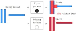
Random defects are the result of contaminants (e.g., dust) present in clean-room manufacturing facilities. A random manufacturing defect, by its very nature, is unpredictable as to when and where it will occur. For instance, a dust speck that lands on a wafer may introduce an extra pattern (creating a short) or cause a pattern to fail or go missing (creating an open), depending on when and where that speck lands. Both results lead to functional failures when the defect occurs in a critical area (Fig. 1).
1. Random defects that occur within critical areas of a layout cause functional failures such as shorts and opens.
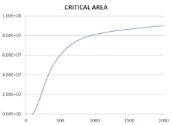
But what, exactly, is this critical area? Critical area is any portion of the layout where a particle of a given size will cause a functional failure (which is why fill shapes are excluded, since they’re non-functional). Critical area depends only on the layout and defect sizes. Not surprisingly, critical area increases as the defect size increases (Fig. 2).
2. Critical area CA(x) in square microns as a function of defect size in nanometers for one defect type, showing the increase in critical area (Y-axis) as a function of defect size (X-axis).
While, in theory, the entire area of the chip could be a critical area for a large-enough defect size, in practice, most foundries limit the range of defect sizes that can be simulated, based on the range of defect sizes they can detect and measure with test chips or metrology equipment.
Defect densities
By accumulating enough data from test and production runs, a foundry can fairly accurately determine the rate of random defect occurrence (defect density) for a specific process. Semiconductor foundries have various proprietary methods for collecting defect density data associated with their manufacturing processes. Test-chip structures usually include what are called “combs and snakes” and via chains (Fig. 3), while optical metrology is another possible source of defect density data.
3. Common test structures used in defect density measurement include snakes, combs, and via chains.
Once a foundry has confidence in its defect density numbers and determined which layers and defect types need to be analyzed, this defect density data is converted into a form compatible with CAA tools created by electronic-design-automation (EDA) companies. In general, a defect density must be available for every layer and defect type for the critical area to be extracted and analyzed. However, in practice, layers that have the same process steps, layer thickness, and design rules typically use the same defect density values.
The most common format is a simple power equation, as shown in Equation 1. In this equation, k is a constant derived from the density data, x is the defect size, and the exponent q is called the fall power. The foundry curve-fits the opens and shorts defect data for each layer to an equation of this form to support CAA.
Defect density data may also be used in table form, where each specific defect size listed has a corresponding density value. One simplifying assumption typically used is that the defect density is assumed to be 0 outside the range of defect sizes for which the foundry has data.
Automated CAA
Using the defect density data provided by the foundry, CAA tools calculate values for both the average number of faults (ANF or Lambda_ANF) and predicted die yield for a design in a given manufacturing process.
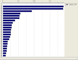
While traditional CAA consists of shorts and opens calculations, some CAA tools also analyze potential via and contact failures. In fact, once CAA is applied to a layout, via and contact failures often prove to be the dominant failure mechanisms during manufacturing (Fig. 4). Other failure mechanisms can also be incorporated into CAA, depending on the defect data provided by the foundry.
4. This chart shows Pareto of ANF values for defect types in a large SoC. The dominant defect type in this analysis is contact to diffusion.
ANF and yield for opens and shorts
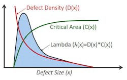
Once the critical area CA(x) is extracted for each layer over the range of defect sizes, the defect density data D(x) is used to calculate ANF according to Equation 2, using numerical integration (Fig. 5).
The dmin and dmax limits are the minimum and maximum defect sizes according to the defect data available for that layer.
5. Visual display of the ANF calculation for opens/shorts.
In most cases, the individual ANF values may simply be added to arrive at a total ANF for all layers and defect types. Note that ANF isn’t strictly a probability of failure, because ANF isn’t constrained to be less than or equal to 1.
Once the ANF is calculated, one or more yield models are applied to make a prediction of the defect-limited yield (DLY) of a design. One of the simplest, most widely used yield models is the Poisson distribution, shown in Equation 3. Of course, DLY can’t account for parametric yield issues, so care must be taken when attempting to correlate these results to actual die yields.
ANF and yield for cut layers
Calculation of ANF and yield for cut layers (contacts and vias) is generally simpler than for other layers. In fact, most foundries define a probabilistic failure rate for all single vias in the design and assume that via arrays don’t fail. This simplifying assumption neglects the problem that a large enough particle will cause multiple failures, but it greatly simplifies the calculation of ANF and reduces the amount of data needed from the foundry. All that’s required is a sum of all the single cuts on a given layer. Then the ANF is simply calculated as the product of the count and the failure rate, shown in Equation 4:
Once the ANF(via) is calculated, via yield may be calculated as described above. Regardless of which yield equation is used, total yield is always a product of the individual yields for each layer and defect type. Vias between metal layers may all use one failure rate, or separate ones based on the design rules for each via layer. The contact layer can be separated into contacts to diffusion (N+ and P+ separately, or together), and contacts to poly, each with separate failure rates.
Use models for CAA
Designers can use CAA on their layouts to ensure that their design methodology, and even purchased intellectual-property (IP) blocks, are compliant with DFM initiatives. When CAA is applied on the design side, it can alert designers to specific layers, defect types, or design elements that might induce manufacturing problems leading to low yield. With CAA, designers get the information about what parts of their design are most sensitive to manufacturing issues, while the foundry has a higher confidence that they will be able to manufacture the design successfully.
Retargeting is a data preparation operation performed on a layout that modifies the drawn interconnect layers to enhance yield and achieve performance targets. When second-source designs must be retargeted for manufacturing, it’s crucial to also analyze them for potential yield limiters before production. Even if multiple designs were all retargeted against the same set of design rules, a foundry can’t be sure that their DFM recommendations were consistently applied to each design originally. Thus, running CAA is a valuable step.
The foundry can also use CAA to screen incoming designs for potential yield limiters before they’re released to production.
DFM Scoring
Automotive and IoT markets have stricter demands on failure rates and reliability than consumer products. Automotive applications typically require six-sigma (6σ) defect rates and 10-year reliability. While some IoT applications may be “throw-away” devices, others may be in locations that are very difficult to access after placement, requiring higher reliability over the expected product life.
In many cases, the foundry provides recommended rules that designers can apply to make their designs more robust against performance and reliability failures. Recommended rules are just that, they detect design conditions that will not impact successful manufacturing, but may affect yield or performance. While recommended rule checking isn’t strictly required like design rule checking (DRC), recommended rules may help designers resolve layout issues related to process variability, parametric yield, or reliability.
Unfortunately, recommended rule checking can report thousands of violations, but the results provide no indication of which errors or types of errors are the most critical to fix, or when the issues have been adequately fixed. To solve that problem, recommended rules are evaluated with DFM scoring decks that return a score against an “optimum” solution, rather than a pass/fail result. Whichever manufacturing challenges are causing the greatest yield loss or poorest reliability can be written into a recommended rule and scored accordingly.
This DFM scoring also allows the foundry to assign a priority-based weighting to the various rules written into the scoring deck. Rules that have minimal impact on the score will be clearly noted, so designers don’t spend time fixing violations that return little benefit. Target scores for the top priority rules give designers achievable goals to meet, and ensure their effort is applied where it will help the most. In addition, results can be put into groups (such as reliability, power, or yield) by the foundry deck writers. With this categorization, designers can selectively view DFM result groups that are more relevant to their market segment.
CAA tools typically produce detailed reports that provide the designer or process engineer with actionable feedback they can use to prioritize debugging. While the contents of these reports vary from one tool to another, displays such as color maps, histograms, and charts, combined with numerical data, help designers quickly pinpoint the most likely opportunities for the greatest improvement.
While CAA is about measuring the sensitivity of a design to random defects, DFM scoring can evaluate yield limiters that aren’t related to random defects. Figure 6 depicts three different configurations for a via between two metal layers. The via on the left is a single via with the minimum metal surround permitted by the DRC rules. The center example is a double via, also with minimum metal. The via on the right is a single via, but with a large metal enclosure drawn according to the recommended rules.
6. Different configurations of vias have different priorities, depending on design priorities and foundry processes.
The question is, which configuration is the best for overall yield and reliability? The answer depends on data from the foundry and the design company’s objectives for their product. In general, the single via on the left is the worst, but in many cases, there’s no room in the layout to use one of the other configurations. The double via may be best if via failure rates are high. If misalignment is a bigger problem, then the large via surround is preferred.
When scoring via configurations, single vias and via enclosures can be scored separately, depending on design priorities. For example, it may be that redundant vias are the best for yield, but larger via enclosures are best for long-term reliability.
DFM Fixing
In DFM fixing, designers need to understand that it’s not possible, or even desirable, to fix all DFM errors. The designers’ goal is to achieve the target score on all of the most critical DFM issues.
Yield-enhancement techniques can be applied to yield and reliability issues separately. It’s possible to add yield-enhancement routines to a DFM scoring deck to provide an automated fixing solution. For example, double vias or rectangular vias can be inserted, and via surrounds can be enlarged, where possible.
Some DFM scoring tools are able to automatically generate DFM scores before and after applying fixes in the same run. The designer can then decide whether or not to keep the layout shapes generated by the DFM scoring deck, or to use them as hints toward improving the layout in some other way to achieve the target score. By putting automated DFM fixing into a DFM scoring deck, the foundries add value to their offering, while ensuring that incoming designs will be successful in manufacturing.
The Tradeoff Between CAA and DFM Scoring
In the ideal case, the foundry provides both CAA and DFM scoring capabilities to the designers, so they can make their designs as robust as possible. In some cases, resource limitations make this difficult. The table shows a comparison between the two in terms of capability and effort.
CAA and DFM scoring tradeoffs
In terms of required effort, DFM scoring requires the foundry to develop a custom rule deck. CAA usually does not, as the rule deck is generated on the fly, although some foundries have developed their own custom CAA rule decks. CAA requires defect densities, DFM scoring does not. The methods of acquiring defect density data are beyond the scope of this article, but suffice it to say that it takes some effort and resources to develop accurate defect densities. If accurate yield prediction isn’t required, then CAA can use estimated defect densities that still provide designers valuable feedback, while minimizing the effort required from the foundry.
In general, CAA decks don’t implement yield-enhancement techniques. DFM scoring decks can easily incorporate automated yield-enhancement routines that allow the tool to report “improvability” scores, or simply score the design before and after improvement. The shapes created by the yield-enhancement routines are saved for review by the designer. The designer can choose to keep them, or discard some or all of the suggested enhancements.
Conclusions
CAA enables designers to predict DLY before tapeout. CAA also allows foundries to screen incoming designs for potential random defect sensitivity, and drives process improvement efforts by reporting layers and defect types to which typical designs are most sensitive. Some foundries even use CAA to drive optical metrology equipment, so that the most detailed inspection effort is applied in the locations where the design has hotspots.
DFM scoring gives layout designers actionable reports that enable them to apply DFM fixing only on the layers and rules that need fixing the most. DFM scoring decks can also provide hints, or make suggested improvements, that the designers can review and merge into the layout to improve their designs. DFM scoring can be used by the foundry to screen incoming designs for potential yield issues.
Foundries, fabless designers, and integrated-device manufacturers are all able to benefit from addressing manufacturing susceptibilities in designs before tapeout and manufacturing. Using a DFM tool provides a single source for CAA and DFM scoring. It also enables automated design enhancement to achieve the best results in both yield and product quality, and can return significant benefits in the form of improved yield and product performance.
Simon Favre is Technical Marketing Engineer at Mentor, a Siemens Business.

