Download this article in PDF format.
For more than three decades, system-level designers have employed FPGAs for multitude of reasons, but the two main factors are performance and flexibility. Many tasks executed in software running on a microprocessor or microcontroller will benefit from significant performance improvements when these tasks are instead implemented in hardware. That path usually leads to either an ASIC/SoC design or an FPGA.
When designing with ASICs and SoCs, however, there’s a caveat. If you’re absolutely certain that there will never be any changes in the associated algorithms, then freezing them into ASIC gates makes sense. These days, not much seems that stable. Standards change. Market needs change. If you freeze the wrong algorithm in ASIC gates, you will need to re-spin the chip.
Consequently, system-level designers often rely on FPGAs to execute algorithms at hardware processing speeds, but with the added flexibility to change the algorithm in milliseconds (or less) if required. Pairing an application processor or microcontroller with an FPGA on a circuit board is now common design practice. The processor runs most of the embedded system’s code and the FPGA accelerates tasks that need more performance than the processor can deliver.
However, communications between the application processor and the FPGA presents a significant bottleneck when the processor and FPGA reside in separate chips. No matter how fast the communications between the two devices, the FPGA is always logically “far away” from the processor when it’s packaged separately and forced to communicate with the processor over PCB traces.
Many chip-to-chip communications protocols have been used to connect processor chips with FPGA chips over the years. At first, parallel connections dominated. Lately, PCI Express (PCIe) has become the most common protocol for connecting processors with FPGAs on PCBs. PCIe is a high-speed serial protocol, which means the data transfers are fast, but the PCIe protocol adds communications latency to serialize the data, transmit it, and then deserialize it.
Embed an FPGA into Your ASIC or SoC
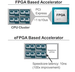
As an alternative, you can embed an FPGA, which then becomes an embedded FPGA (eFPGA), into your ASIC or SoC as a programmable accelerator. When you do that, you can directly connect the communications paths in your ASIC to the eFPGA’s routing structure. This direct connectivity reduces the communications latency from 1 to 10 µs for PCIe down to something on the order of 10 ns (Fig. 1).
1. Embedding an FPGA into your ASIC reduces the communications latency between CPU and FPGA to approximately 10 ns, a 100X improvement compared to the latency between separately packaged processors and FPGAs.
Instantiating one or more eFPGAs into your ASIC or SoC breaks the communications bottleneck. You can instantiate as much connectivity between on-chip processor(s) and on-chip eFPGA(s) as required by your application(s).
For example, many SoC designs couple Arm processor cores to other on-chip hardware using Advanced eXtensible Interface (AXI) buses. You can easily use a 128-bit AXI bus to connect a complex of processors to an eFPGA. But why stop there? If your application requires more bandwidth, you can use two, four, or more 128-bit AXI buses to drive multiple accelerators instantiated in the eFPGA(s).
There’s another, more subtle reason why eFPGAs outperform discrete processor/FPGA implementations. Because a separately packaged FPGA is logically “far away” from the processor, it must usually have its own attached SRAM or double-data-rate (DDR) SDRAM to buffer large data blocks.
That means the processor or a direct-memory-access (DMA) controller must move the data to be processed from the application processor’s DDR SDRAM to the FPGA’s SRAM or DDR SDRAM. Then, the processed data must be transferred back from the FPGA’s SRAM or DDR SDRAM to the processor’s DDR SDRAM. Depending on the amount of data to be transferred, the delay incurred by these data transfers falls somewhere between a long, long time and forever (from a hardware-level speed perspective).
Given on-chip eFPGA direct access to the processor’s main memory, data needn’t be transferred between the processor and the eFPGA. A large data transfer therefore becomes nothing more than passing a pointer to the eFPGA so that it can immediately start processing the data where it already resides in shared memory. When the eFPGA completes its work, it passes a memory pointer for the processed data block back to the on-chip processor for any additional handling.
Using an eFPGA essentially cuts the system power consumption devoted to a packaged FPGA by half because the eFPGA dispenses with the die area associated with the programmable I/Os, which are almost always found in a packaged FPGA. Because the eFPGA resides on the ASIC’s or SoC’s die and communicates directly with other on-die IP blocks, an eFPGA doesn’t need complex programmable I/O structures to provide level translation and other sorts of I/O flexibility. Other circuitry on the ASIC or SoC don’t require this sort of flexibility.
Costs associated with the eFPGA’s die area are therefore significantly smaller than for a packaged FPGA because the eFPGA requires significantly less die area. Other costs are eliminated or reduced (including the cost of the FPGA package), no additional PCB space for the FPGA is required, and fewer support components are needed, such as the multiple local power-supply regulators normally required by packaged FPGAs.
eFPGA Architecture and Custom Blocks
Column-based architectures have long been established as the most efficient way to lay out FPGAs. A column-based FPGA architecture organizes different functions into separate columns. So there will be one or more columns for the lookup tables (LUTs), one or more columns for the memories, and one or more columns for the DSP cores. The eFPGA’s programmable interconnect surrounds the columns.
In packaged FPGAs, the FPGA maker determines the mix of these different functions. Because packaged-FPGA vendors design their parts to serve a broad audience, it’s difficult to get a packaged FPGA that truly suits any specific application’s unique requirements. However, when you incorporate an eFPGA into an ASIC or SoC, you determine the optimum functional mix of predesigned columns as required by your intended application(s).
There’s another, more important difference between packaged FPGAs and eFPGAs. You’re not limited to standard functional columns (LUTs, memories, and DSPs) when you design your eFPGA. You can develop custom blocks that will improve performance for specific tasks and will further reduce die size.
Custom Blocks Improve Performance
The following eFPGA example, based on an Achronix Speedcore eFPGA, illustrates the performance benefits of custom blocks. The application in this example is 400-Gb/s wireline packet processing. This sort of extreme speed is really tough to achieve with eFPGAs because it is very difficult to close design timing for data streaming through any eFPGA or FPGA at 400Gbps. Any hope for success at these speeds demands very wide internal buses within the FPGA design – as wide as 1024 or even 2048 bits.
However, custom eFPGA blocks give you the ability to put the application’s highest-speed data through ASIC gates instead of the eFPGA’s LUTs and programmable interconnect. The eFPGA simply implements the more specialized packet-processing tasks, which require less bandwidth.
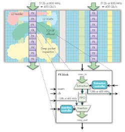
In this example, a custom block for packet extraction (PX) and insertion (Fig. 2) can be designed to handle the high-speed, 400-Gb/s packets. The logic implemented in the eFPGA then commands the PX blocks to capture and extract specific portions of the packets, such as the packet header. Subsequently, the programmable portions of the eFPGA are able to process these extracted packet bits and re-introduce modified packet blocks back into the packet flow later in the PX pipeline.
2. Adding custom packet-extraction blocks to the eFPGA allows it to handle 400-Gb/s packet traffic, which wouldn’t be otherwise possible without extremely wide (1024-bit or 2048-bit) buses, if at all.
Use of custom eFPGA blocks allows you to realize the kind of performance that today’s standalone FPGAs simply cannot attain.
FPGA design implementations are fundamentally inefficient compared to ASIC implementations, by a factor of 10X or more. That’s simply the engineering tradeoff you make in exchange for the FPGA’s programmability and flexibility. Embedding an eFPGA infuses an ASIC with that same sort of programmability and flexibility, but you certainly don’t want to give up all of the efficiency you get from designing an ASIC in the first place.
Custom blocks allow you to better exploit an eFPGA’s flexibility where you really need it, while reducing the other portions of your design—the parts that will not change—to more efficient but unchanging ASIC gates. By using some of these ASIC gates to implement functions as custom blocks within the eFPGA’s fabric, you can get the speed you need where you need it and still achieve the eFPGA’s flexibility and programmability where it really matters.
FPGA vs. eFPGA: The Real Differences
If you look at the die photo of a standalone, packaged FPGA, you’ll see that the FPGA core (the LUTs, memories, and DSPs) consumes only about half of the total die area. The other half is dedicated to the FPGA’s programmable I/O circuitry.
In the packaged FPGA domain, the programmable I/O is the real secret sauce. A packaged FPGA’s programmable I/O circuitry allows system designers to connect the FPGA to almost any other device, including microprocessors, memory, ASICs, and even other packaged FPGAs. That’s why an appropriate amount of a packaged FPGA’s die area is allocated to I/O. An eFPGA doesn’t have or need the programmable I/O of a packaged FPGA, because it’s connected directly to other on-chip blocks.
In addition to the extra area absorbed by the on-chip programmable I/O in a packaged FPGA, the programmable I/O circuitry consumes a large chunk of the packaged FPGA’s total power. Like the extra die area, the extra power consumed by the programmable I/O circuitry is also absent when using an eFPGA.
Next, there’s the hardware “shell.” Many FPGA-based hardware accelerator designs have a standard hardware shell, which is the portion of the design, usually the system interface, which doesn’t change from one design iteration to the next. For example, a hardware accelerator’s processor interface generally will not change from one generation or one design to the next. Only the functions inside of the shell change. Consequently, the shell needn’t be, and shouldn’t be, implemented within the programmable eFPGA because the flexibility isn’t needed. Implementing shell functions with ASIC gates improves performance and shrinks die area.
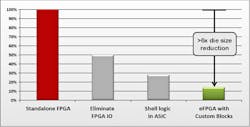
The net result is that custom blocks designed into your eFPGA could require as little as one-sixth the die area that would be needed when implementing the same function in a standalone, packaged FPGA (Fig. 3).
3. Using custom eFPGA blocks, eliminating the programmable I/O used in packaged FPGAs, and hardening shell functions in the ASIC can cut the size of the eFPGA block to less than one-sixth of the die area required by a packaged FPGA.
In summary, the option to add custom blocks to an eFPGA design is critical to the efficient use of an ASIC’s die area and to achieving performance goals while retaining the desired flexibility through hardware programmability.
Steve Mensor is Vice President of Marketing at Achronix Semiconductor Corp.


