>> Electronic Design Resources
.. >> Library: Article Series
.. .. >> Series: Path to Systems
The previous articles of this series have discussed the innovation and evolution of the integrated-circuit industry and how system-in-package (SiP) devices fit into the market. In the first article, Path to Systems: Opportunities and Challenges for the Next Generation of Semiconductor Integration, we looked at how the ability to integrate more transistors at a lower cost, increase performance, and lower power dissipation has revolutionized not only the semiconductor industry, but all industries who have been able to take advantage of silicon devices.
In Path to Systems: Why a SiP?, we walked through the underlying technology of a SiP, using the Octavo Systems OSD335x-SM as an example and exploring how SiP technology is taking on a role as a complementary capability to further drive industries creating and using semiconductor technology. Then in Path to Systems: SiP—Leveraging Mass Production on a Small Scale, we explored issues and opportunities resulting from this emerging technology. We evaluated the design and production flows of SiP technology, delving into the example of the 100-Plus-Component-OSD335x C-SiP, a complete computer in a package.
Finally, because of the advantages a SiP brings to all stages of a system production from design to manufacturing and testing, in Path to Systems: A SiP of Reliable Advantage–Systems Under Test we highlighted the importance of creating the tools and processes to allow for the industry to utilize SiP technology.
In this article, we look toward the future of system-in-package, in which new tools and processes provide a system designer with capabilities to customize SiP devices while maintaining low design and manufacturing costs. From customer-selectable sub-modules to SiPs within SiPs, we begin to glimpse the ultimate system-in-package.
Creating a System-Specific SiP
Two major advances need to be made to give the system designer the ability to create system-specific SIP devices:
• The creation of a design methodology to allow for semi-custom and custom SiPs.
• The creation of a manufacturing flow that will allow for low-volume manufacturing of SiP devices.
The Design Methodology
The concept of a “system in a package” implies that it’s an integration of different components rather than the creation of a single component. While this concept doesn’t eliminate the need for new individual components, it changes the role of component design. Given that individual components will be integrated together within the SiP, we need to think about and design “SiP-ready” components rather than just standard components, such as a traditional system-on-chip (SoC).
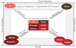
The design methodology for SiPs borrows from traditional SoC design as well as printed-circuit-board (PCB) design and shifts semiconductor manufacturers’ focus from traditional methods of designing single monolithic components to designing systems with several interconnected components. For example, instead of trying to cram as much as possible into a single SoC, it would be better to split components along silicon process lines—analog components in optimized analog processes, digital components in optimized digital processes, RF components in optimized RF processes, and power components in optimized power processes (Fig. 1).
1. Moore’s Law has caused semiconductor processes to progress in multiple directions.
By taking advantage of the process improvements generated by Moore’s Law, not only can we use better components, we also reduce “wasted” silicon because we need only integrate the components necessary for the system. In addition, to realize the potential of SiP technology, we will not only need to define the interfaces between “SiP-ready” components, but create tools and processes that will allow us to partition a system so that the best aspects of SiP technology and silicon technology are utilized.
Beyond changes to the design methodology for component manufacturers, customers also must shift their design methodologies to better utilize SiP technology. As SiP devices become more customizable, the ability to generate schematics, layout, and a bill of materials for a custom SiP based on as product specification becomes paramount. Furthermore, the ability to prototype with SiP will need to be understood and integrated into the product design process.
The Manufacturing Flow
Just as the move from monolithic components to integrated systems impacts the design methodology, it will also require adjustments in the manufacturing flow. Today, high-volume SiPs can be manufactured with the same process as a standard semiconductor component. This is both good news and bad news. The good news is that the component manufacturing process has had many decades of optimization to maximize yield, maximize throughput, and minimize manufacturing costs. The bad news is that none of these characteristics (yield, throughput, and cost) lend themselves to the low-volume manufacturing required by a custom SiP.
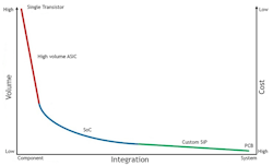
Figure 2 shows the relationship between integration and volume. At one end, we have extremely high-volume components that are fixed-function and integrate relatively little of the system. At the other end, we have complete systems that integrate all components but have a much lower volume. Given that manufacturing processes have been optimized for high volumes, this means that the cost per unit increases as the volume decreases.
2. The number of transistors in a device vs. volume of device.
Ideally, we would like to integrate a custom SiP with the low cost of manufacturing of a high-volume component. We believe that this can be achieved with innovation around customizable SiPs. Given the programmability of today’s manufacturing, assembly, and test machines, we see that it will be possible to reduce the economic manufacturing volume from millions of units to a single unit. Just as stencils are being replaced with programmable solder-paste printers to reduce the cost of small-volume PCB manufacturing today, programmable wire bonders, pick-and-place machines, and testers will usher in an era of increased integration and reduced cost at small volumes.
What’s Driving SiP Technology Today?
Traditionally, the driving force for SiP technology has been the demand to place more components into a given PCB area to allow for smaller form factors. By utilizing tighter place-and-route rules and unpackaged die, SiPs were able to integrate components of a system much more efficiently than on a PCB. In addition, SiPs were able to even utilize the third dimension using techniques like stacking die or in-substrate passives. However, this demand and ability has been driven by large volumes and require large upfront investments.
Fortunately, thanks to lowering cost for SiP technology, i.e. smaller volume requirements and initial investment, we’re seeing system simplification become a driving force behind SiP technology. The desire to simplify a system design by abstracting parts of it away, enabling designers to focus on the key parts of their systems, has become as important, if not more important, than packing components into a given volume.
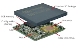
As design and system complexity grow while design teams shrink, the need for easy-to-use components that integrate the tedious, non-value-added portions of the design becomes critical. For example, in a microprocessor-based system, the connections between the processor, power management, and high-speed memory are the same every time for a given microprocessor. Figure 3 shows a SiP, which integrates a TI AM3358 microprocessor, DDR3 high-speed memory, and the power management integrated circuit (PMIC), that greatly simplifies the end system design.
3. Shown is a tightly integrated Texas Instruments AM335x-based system-in-package—the OSD335x from Octavo Systems.
As the demand for system-level integration and simplification ramps up, the components of today will become “SiP-ready” components while the SiPs of today will become “sub-system in packages (S-SiPs)”. S-SiPs and SiP-ready components will be integrated into larger SiPs as system integration drives SiP technology toward the ultimate SiP.
The Ultimate SiP
Given the changes in design and manufacturing required to utilize SiP technology, we should ask ourselves: “What would be the ‘Ultimate SiP?’” The simple answer is a component with zero pins. It’s a custom component that completely performs the intended function without the need to be physically connected to anything else. It can communicate wirelessly, create or harvest its own energy, and perform its necessary functions autonomously. And it’s cheap to manufacture, can operate in harsh conditions, and requires little maintenance.
By integrating all of the system’s components into a single package, we rid ourselves of many of the challenges we face today as we struggle to build systems. Instead of focusing on the “how do I make XYZ work?,” SiP technology will free you to focus on the “what about …?” as system design transitions from a select few implementers to the many dreamers where creativity begins by first asking the right questions.
Conclusion
Even with the slowdown in the ability to shrink transistors, there appears to be a great future ahead in the world of semiconductor integration. We can see the continuation of Moore’s Law as it begins to focus on system integration where we integrate using silicon rather than on silicon. With the capabilities provided by system-in-package, there’s no end to the number of transistors we will be able to integrate into an IC package. So, the next time you look to design a system, ask yourself: “Is there a SiP for that?”
- Series: Path to Systems
- Prior article in this Series ... A SiP of Reliable Advantage—Systems Under Test
References:
https://imapsource.org/doi/abs/10.4071/2380-4505-2018.1.000019


