Universal Asynchronous Receiver/Transmitters (UARTs) are considered the simplest way to send data from one system to another system. UARTs are commonly included in microcontrollers and many modern ICs now come with a UART that can also communicate synchronously, called Universal Synchronous/Asynchronous Receiver/Transceiver (USART).
Along with the widespread use of UARTs in systems, it is also necessary to test the interface to verify that it is compliant with the standards. The following tests are usually done on the UART hardware/IP of the Device-under-test (DUT) at varying baud-rate, data, parity, and stop bit widths.
- Basic loop back test
- Standard UART transmit and receive tests
- Parity and framing error conditions
- UART transmit and receive with LSB/MSB first options
- Timing tolerance test
Except for the basic loop back test, the other cases require a special validation platform to check the DUT’s compliance with the standard UART interface. It can be seen that such a platform is not available off-the-shelf for immediate use. Companies testing their UART design usually make a custom validation suite, test manually, or use standard interface ICs or USB-UART bridges available in the market. However, all these offer only limited test coverage.
This article introduces a generic UART validation automation platform that can be used to test all aspects of UART interfaces in an automated way.
A Standard UART Frame
The standard UART frame definition (Fig. 1) addresses the range of UART specifications.
The start bit (low for 1 bit duration) does not change across different versions of UART frame standard. Other fields of the frame change length based on the application. Devices support a data width as low as 4 bits up to a maximum of 9 bits per frame. In some special cases, when required by design, the data width takes an arbitrary value keeping other parameters compliant, but not necessarily compatible with standard UART interfaces. A parity bit can be introduced when error checking is required. At best it can detect a single bit error at the receiver end. The stop bit (high till start of next packet) may be one or more bits. Multiple, possibly partial bits, may be used to allow the receiver time to process the incoming data.
The UART Validation Platform
A robust UART validation platform must test all the features of the communication interface. It needs to be capable of handling all possible combination of UART parameters in an automated way. Manual UART validation tests are done using manual test cases that require a dedicated resource throughout the test and consume a lot of time. This effort can be reduced by automating the process using a UART Validation Automation Platform that can run repeated tests.
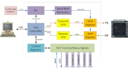
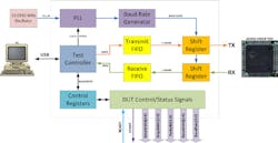
Off-the-shelf tools for testing UARTs do not typically support many of these for the UART frame such as data widths other than 7- or 8-bits or 2.5- to 4.0-bit stop widths. A new validation platform is required, which supports all and even more possibilities. The UART Validation Automation Platform (Fig. 2) described in this article supports the following configurations:
- Baud rate (bits/s): 50, 110, 300, 600, 1200, 2400, 4800, 9600, 19200, 28800, 38400, 57600, 115200, 230400, 460800, 921600
- Data width (bits): 1, 2, 3, 4, 5, 6, 7, 8, 9, 10
- Parity bits: none, odd, even
- Stop bits: 1.0, 1.5, 2.0, 2.5, 3.0, 3.5, 4.0
- Transmit buffer size: 16 frames
- Receive buffer size: 16 frames
The Test Controller is the heart of the validation platform. This is an MCU (micro control unit) used to collect, manipulate, and forward the data between other blocks in the system. It should have a USB interface to talk to a host computer.
The Transmit and Receive FIFO handles the data frames to be transmitted are stored in the Transmit FIFO and data frames received from the DUT are stored in the Receive FIFO. The MCU collects transmit packets from the host, converts them into frames, and loads them into the transmit FIFO. The receive FIFO forwards the frames collected from the DUT, forwards them to the Test Controller for packet conversion and relaying to the host. Buffering data packets is a good approach to improve the speed of the system.
FIFOs are implemented in SRAM on the MCU. This implementation supports only 16-frames per transmit or receive session. It can be increased based on individual requirements and is limited by available SRAM.
Shift registers (Parallel-to-Serial and Serial-to-Parallel converters) are used for transmitting and receiving data. Both registers are clocked at double the baud rate frequency or multiples of the frequency.
The packet to be transmitted is already available in the FIFO, converted as frame bits. This frame data is loaded into the Transmit Shift Register and sent across to the DUT at the correct baud rate. A similar approach is used for receiving packets from DUT. The received frame is sampled at two times the baud rate (or more) and this frame bits are moved to the receive FIFO once the full packet is in the receive shift register.
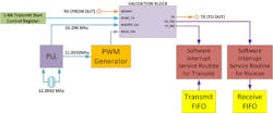
The PLL (phase lock loop) and the Baud Rate Generator generate the clock frequency used by all other blocks. The PLL block uses an external 11.0592 MHz crystal oscillator, It multiplies the input clock by a factor of five to generate the 55.296 MHz master clock frequency. Since all blocks are operated with the same clock source, there is no extra need to use extra logic to synchronize the blocks.
The external oscillator is selected to generate the precision baud rates required for a generic UART application. The 11.0592 MHz clock source can be divided to make standard baud rate clocks for the shift registers. The baud rate generator serves this purpose. A digital PWM block is used to generate the baud rate clock. The period and compare parameters of the PWM are varied to generate the baud clock at 50% duty cycle. Variable duty cycles are another advantage of using a PWM block instead of clock dividers that generate only fixed duty cycle outputs. A variable duty cycle may be used to validate the clock tolerance and output fidelity of the UART interface being tested.
All parameters and settings are stored in 8-bit control registers. The test controller’s SRAM can be used for this purpose. The host computer can read or write these registers via the same interface used to access the FIFOs. The following registers are available for this platform
Control register: Immediate commands are communicated using this register. The MSB of this register is used to inform the Test Controller about a new command in this register. This bit is cleared after executing the command. The commands supported and their corresponding values are as follows.
|
Command |
Register Value |
|
Change Configuration |
0x01 |
|
Get Status |
0x02 |
|
Set Baud Rate |
0x03 |
|
Set Data Width |
0x04 |
|
Set Parity Bit |
0x05 |
|
Set Stop Bits |
0x06 |
|
Set Oversample Rate |
0x07 |
|
Set TX Frame |
0x08 |
|
Set TX Data |
0x09 |
|
Get RX Data |
0x0A |
|
Get RX Size |
0x0B |
|
Prepare DUT |
0x0C |
Status register: The test controller uses this register to publish the outcome of the current test, including error conditions during transfers.
|
Bit field |
Description |
|
Bit-0 |
Data transmitted (1), Data pending transmission (0) |
|
Bit-1 |
Data received (1), Data pending reception (0) |
|
Bit-2 |
Parity Error (1), No Parity Error (0) |
|
Bit-3 |
Framing Error (1), No Framing Error (0) |
|
Bit-4 to Bit-6 |
Not used |
|
MSB (Bit-7) |
Test complete (1), Executing (0) |
Baud Rate register: This register controls the baud rate used for the next data transfer. The supported baud rates and their values are shown below.
|
Baud Rate |
Register Value |
|
50 |
0x00 |
|
110 |
0x01 |
|
300 |
0x02 |
|
600 |
0x03 |
|
1200 |
0x04 |
|
2400 |
0x05 |
|
4800 |
0x06 |
|
9600 |
0x07 |
|
19200 |
0x08 |
|
28800 |
0x09 |
|
38400 |
0x0a |
|
57600 |
0x0b |
|
115200 |
0x0c |
|
230400 |
0x0d |
|
460800 |
0x0e |
|
921600 |
0x0f |
Data Width register: This register controls the data width used in the next data transfer. Supported values are 0x01 to 0x0A (10 values).
Parity Bit register: The parity bit is set using this register. It can be none, odd, or even as shown below.
|
Parity |
Register Value |
|
No Parity |
0x00 |
|
Odd Parity |
0x01 |
|
Even Parity |
0x02 |
Stop Width register: This register specifies the stop width to be used with each frame. The supported stop widths are given below.
|
Stop Width |
Register Value |
|
1.0-Bit |
0x00 |
|
1.5-Bits |
0x01 |
|
2.0-Bits |
0x02 |
|
2.5-Bits |
0x03 |
|
3.0-Bits |
0x04 |
|
3.5-Bits |
0x05 |
|
4.0-Bits |
0x06 |
Over Sample Rate register: The amount of oversampling required for transmit and receive frames is specified using this register. Logic complexity increases with the oversampling rate required. The minimum value is two.
TX (transmit) Size register: This register holds the number of transmit frames in the FIFO. The value is either set manually after loading the transmit FIFO with data or automatically loaded when the FIFO is loaded. Maximum value is 16 and minimum is 1.
RX (receive) Size register: This register holds the number of transmit frames in the FIFO. The value in this register is incremented by 1 when a frame of data is received and decremented by 1 when the host reads a frame from the FIFO. Maximum value is 16 and minimum is 1.
DUT (device under test) Control and Status Signals register: The data includes parameters that is to be communicated to the DUT. This block gets the parameters from the control registers and pushes it to the DUT. A parallel interface is used to inform the DUT about the current settings. Additionally, the platform has a control signal, “START”, which is asserted to initialize the DUT. Another signal, “READY”, is asserted by the DUT when it has applied the settings from platform and is ready to start the test.
The host computer executes a Perl script for the tests and communicates with the platform through the USB port. All test cases are implemented as a Perl script, which generates the test sequences to cover the validation. It also collects the data to check whether the test is a pass or fail. This information, along with the test case, is written to a file for logging purposes.
The DUT is the target device with UART interface to be tested.
The Frame Validation Block
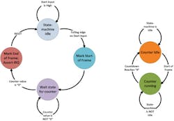
The Frame Validation Block (FVB) provides the logic to detect the start of a frame and its length. The operation of the FVB is specified by a state machine (Fig. 3).
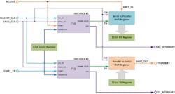
The FVB can be shown as a block diagram (Fig. 4) with these inputs and outputs:
- CLK_IN (input): This is the master clock. The frequency of this clock must be higher than the baud clock. The falling edge of the START input is sampled and detected using this clock.
- BAUD_CLK (input): This is baud clock frequency multiplied by the oversample rate. Minimum value of the clock input is twice the baud frequency.
- START (input): A falling edge on this input denotes the start of the state-machine.
- COUNT (input): This is an 8-bit frame width used to initialize the countdown timer period.
- FRAME_VALID (output): This output signal goes high at the falling edge of the START input and goes low when the counter times-out.
- IRQ (output): A rising edge on this output denotes the end of one frame. It goes high for one master clock period when the counter times-out. Its value is reset to ‘0’ when the state-machine returns to idle state.
The UART Validation Block
The UART Validation Block (Fig. 5) is built from a pair of VFBs. The Start input for the receive frame validation block is the RX input. Since transmitting a frame is under our control, the START input to its frame validation block (FVB) is sourced from a single-bit register.
The count register is shared between the TX and RX frame validation blocks since the transmitted and received packets are of the same width. The frame valid signals from these blocks are used as an enable signal for the respective section’s shift register. As explained before, the transmit section uses a parallel-to-serial converter while the receive section uses a serial-to-parallel converter. Both these converters have access to a 32-bit memory location to store a single frame and have shift-left implementation. During initialization, both registers are padded with ‘1’s
The UVB is connected to the input, outputs, and other top-level blocks (Fig. 6). The baud clock for the UART Validation Block is generated using a PWM unit. It is used to create the required clock frequency from the fixed 11.0592 MHz input clock, acting as a frequency divider. The output frequency of the PWM unit is decided using the required baud rate and the oversampling rate for the validation block. The period and compare values of the PWM unit are varied to generate the require clock frequency. The same block may be used to generate clock jitter and variable duty cycle clocks for validating the DUT’s tolerance to baud rate variation. All possible real-life scenarios can be emulated using this feature of the validation platform.
The interrupt request (IRQ) outputs from the validation blocks are associated with two software interrupt service routines (ISR) – one each for transmit and receive. These ISRs handle transmit and receive FIFOs. At the end of transmitting a frame, the transmit ISR is invoked to load the next frame from FIFO into the transmit shift register. Similarly, when a frame of data is received, the receive IRQ takes the contents from the receive shift register and push into the receive FIFO.
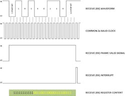
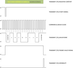
Figure 7 shows a typical timing diagram for a receive event, and Figure 8 shows the timing diagram for a transmit event. All the signals involved during both these phases are also included in the figures. Both cases assume an 8-bit data with no parity bit and 1.5-bit stop width for the UART packet. Also, for simplicity, oversampling rate is considered as two (2), i.e. the baud clock is twice the actual baud rate frequency. The valid frame data in the register contents is marked in yellow since the data is padded with ‘1’s during initialization to fill the 32-bit shift registers.
System Firmware
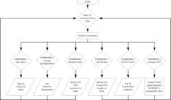
The test controller system provides commands and data to test a system (Fig. 9). It stores the frames to be transmitted and frames received from the DUT in a FIFO implemented in SRAM. The interrupt service routines (ISR) for handling transmit and receive packets are also implemented in the MCU, using its generic IRQs. The basic flow is shown in the flowchart in Figure 9.
System Software
The host is a Windows PC running tests written using the Perl Scripting Language. The USB interface library required by the platform is reused from a standard USB-I2C Birdge library for Perl, developed and distributed along with PSoC Programmer software. The “I2C_Lib.pl” Perl library, shipped with PSoC Programmer in examples folder, is used as the hardware abstraction layer for the software. For more details on this interface and library refer to the PPCLI and PPCOM interface documentation included in the PSoC Programmer package. A UART Validation Library was written on top of the hardware driver layer to support communicating with the platform.
The UART Validation Library supports the following APIs.
- Platform_Start(): Must be called before any operation; starts the interface.
- Platform_Stop(): Must be called before exiting from main script; Stops the interface and shows the last communication error message (if any).
- Platform_GetSupportedBaud(): Returns a list of supported baud rates
@BaudArr = (50, 110, 300, 600, 1200, 2400, 4800, 9600, 19200, 28800, 38400, 57600, 115200, 230400, 460800, 921600);
- Platform_ReportError($_): Sets the error value to a global variable, used to determine the last error
$Plaform_LastError = $_[0];
- Platform_CheckPassFail($_): Pass if input is 1, else fail
my $str;
if ($Plaform_LastError !~ /^\s*$/)
  { print time, ": ", $Plaform_LastError . "\n"; }
if (I2C_Lib::SUCCEEDED($_[0]))
  { print time, "Test Successful!\n";}
else
{ @str = ("Test Failed! ", $Plaform_LastError, "\n"); print time, ": ", @str;}-
Platform_COMMAND($_): Sends a command to the Platform from the supported list
my $deviceAddress = $Platform_Address;
print time, ": Sending COMMAND:", $_[0], " to Platform\n";
#Send the Command to Platform
@dataIN = (0x00, 0x80 | $_[0]);
$hr = I2C_Lib::I2C_WriteData($deviceAddress, @dataIN);
if (not I2C_Lib::SUCCEEDED($hr))
  { $m_sLastError = I2C_Lib::GetLastError(); return $hr; }
select(undef,undef,undef,0.1);
return $hr;
-
Platform_WriteConfig(): Send the entire packet from script to MCU. Parameters shall be set using additional APIs before sending the configuration
my $deviceAddress = $Platform_Address;
my $dataIN;

#Send the New Configuration data to Platform
@dataIN = GetBufferAsList();

my $size = @dataIN;
print time, ": ", "Write ", CONFIG_PACKET_WIDTH, " bytes: ";
for(my $i = 1; $i < $size; $i++)
{
  printf("%02X ", $dataIN[$i]);
}
print("\n");

$hr = I2C_Lib::I2C_WriteData($deviceAddress, @dataIN);
if (not I2C_Lib::SUCCEEDED($hr))
  { $m_sLastError = I2C_Lib::GetLastError(); return $hr; }

#Send the Ready-to-Configure command to Platform
$hr = Platform_COMMAND($COMMAND->{COMMAND_ChangeConfig});
return $hr;
-
Platform_ReadConfig(): Displays the current configuration from the MCU
my $deviceAddress = $Platform_Address;
my $dataIN;
my $resArr;
my $arr;

#Initialize the Buffer pointer to beginning
@dataIN = (0x00);
$hr = I2C_Lib::I2C_WriteData($deviceAddress, @dataIN);
if (not I2C_Lib::SUCCEEDED($hr))
  { $m_sLastError = I2C_Lib::GetLastError(); return $hr; }

#Read bytes from device
@resArr = I2C_Lib::I2C_ReadData($deviceAddress, CONFIG_PACKET_WIDTH);
if (not I2C_Lib::SUCCEEDED($hr))
  { $m_sLastError = I2C_Lib::GetLastError(); return $hr; }
($hr, @arr) = @resArr;
my $size = @arr;
print time, ": ", "Read ", CONFIG_PACKET_WIDTH, " bytes: ";
for(my $i = 0; $i < $size; $i++)
{
   printf("%02X ", $arr[$i]);
}
print("\n");
return ($hr, @arr);
-
Platform_CopyConfig(): Copies the MCUs configuration to the local Script buffer. Also displays the values that were copied.
-
Platform_SetBaudRate($_): Sets the Baud Rate value in the local buffer; will not send the value to MCU until Platform_WriteConfig() is called.
$EZI2C_Buffer->BaudRate($_[0]);
-
Platform_SetDataWidth($_): Sets the Data Width value in the local buffer; will not send the value to MCU until Platform_WriteConfig() is called.
$EZI2C_Buffer->DataWidth($_[0]);
-
Platform_SetParityBit($_): Sets the Parity Bit value in the local buffer; will not send the value to MCU until Platform_WriteConfig() is called.
$EZI2C_Buffer->ParityBit($_[0]);
-
Platform_SetStopWidth($_): Sets the Stop Width value in the local buffer; will not send the value to MCU until Platform_WriteConfig() is called.
$EZI2C_Buffer->StopWidth($_[0]);
-
Platform_SetOverSampleRate($_): Sets the Over Sampling value in the local buffer; will not send the value to MCU until Platform_WriteConfig() is called.
$EZI2C_Buffer->OverSampleRate($_[0]);
-
Platform_SetTXSize($_): Sets the number of frames to be transmitted in one session; will not send the value to MCU until Platform_WriteConfig() is called.
$EZI2C_Buffer->TXSize($_[0]);
-
Platform_GetRXSize($_): Returns the number of frames in the RX buffer
return $EZI2C_Buffer->RXSize;
-
Platform_SetRXSize($_): Sets the number of values to be read from PSoC3’s RX Buffer in the local buffer; will not send the value to MCU until Platform_WriteConfig() is called.
$EZI2C_Buffer->RXSize($_[0]);
-
Platform_SetTXDataArray(@_): Sets the data frames to be transmitted in one session. This API overrides the value set (if any) using Platform_SetTXSize($_) API; will not send the value to MCU until Platform_WriteConfig() is called.
@arr = @_;
$size = @arr;
print time, ": SetTXDataArray", $_[0], "\n";
for ($count = 0; $count < $size; $count = $count + 1)
{
  SetTXDataElement($count, $arr[$count]);
}
Platform_SetTXSize($size);
return 0;
-
Platform_GetStatus(): Gets the status register value from the Platform firmware, sets the local status variable and returns the value
my $status;
Platform_COMMAND(2);
($hr, @status) = GetRemoteBufferValue(0x01, 0x01);
$EZI2C_Buffer->Status($status[0]);
return $EZI2C_Buffer->Status;
-
Platform_IsDUTReady(): Returns 1 if DUT is free and 0 if DUT is busy.
my $status;
$status = Platform_GetStatus();
if ($status & STATUS_DUT_READY_MASK)
{
  print time, ": DUT is free now!\n";
  return 1;
}
else
{
  print time, ": DUT is not ready yet!\n";
  return 0;
}
Hardware Implementation
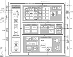
Most of the logic used to implement the UART Validation Automation Platform is contained in a Cypress Semiconductor Programmable System on Chip (PSoC) that includes a microcontroller and configurable analog and digital blocks (Fig. 10). The latter allows the validation hardware to be contained on-chip.
The Universal Digital Blocks (UDB) are configurable program logic arrays (PLA). The PSoC families have 24 UDBs, each consisting of 8 macrocells. These PLA can implement 16 product terms. They also have a datapath cell, a control cell and a status cell. This puts the PSoC configurable components on par with mid to higher end CPLDs like Altera’s MAXV series and Xilinx’s Cool Runner series.
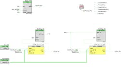
PSoC devices are configured using PSoC Creator. The configuration is located when the system boots. This provides the core CPU with access to customized peripherals. In this case, the UART validation hardware. The PSoC Creator schematic for our UART validation hardware (Fig. 11) is very close to the logic design already presented. This includes the the baud rate PWM, 32-bit shift registers, and the frame validation blocks for both transmit and receive sections.
Baud_PWM generates a clock at double the Baud-rate selected. This ensures correct sampling of data. ShiftReg_TX and ShiftReg_RX are 32-bit shift-registers to handle the TX and RX packets respectively. Start_TX is a 1-bit control register to indicate the start of a TX frame, controlled by firmware. FrameWidth component stores the expected frame-width in number of bit, considering double sample rate. StartTest output pin communicates the start of test to the DUT, which is acknowledged with a rising edge on Ready input pin. Other IOs are used to pass configuration parameters to the DUT before the test begins.
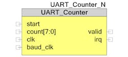
The UART_Counter_TX and UART_Counter_RX are custom designed components in Verilog (Fig. 12). These are implemented using a UDB. This includes the Frame Validation State-machine discussed earlier.
The definition of Frame Validation State-machine in Verilog module is provided below. This does not include the module declaration. However, The Frame Validation Block section discussed and explained the inputs and outputs to this module in detail.
reg valid_reg;
reg start_reg;
reg baud_clk_reg;
reg irq_reg;
reg [7:0] dwn_cntr;
reg [1:0] state;
wire start_fall;
wire baud_clk_rise;
assign valid = valid_reg;
assign start_fall = (~start) && start_reg;
assign baud_clk_rise = baud_clk && (~baud_clk_reg);
assign irq = irq_reg;

always @(posedge clk)
begin
  start_reg = start;
  baud_clk_reg = baud_clk;
    case (state)
  0:begin
      valid_reg = 0;
      irq_reg = 0;
      dwn_cntr = count;
      if (start_fall) begin
        state = 1;
      end
    end
  1:begin
      irq_reg = 0;
      if (baud_clk_rise) begin
        dwn_cntr = dwn_cntr - 1;
        valid_reg = 1;
      end
      else begin
        valid_reg = 0;
      end
      if (dwn_cntr == 0) begin
        state = 2;
      end
    end
  2:begin
      irq_reg = 1;
      valid_reg = 0;
      state = 0;
    end
  default:begin
      irq_reg = 0;
      state = 0;
      valid_reg = 0;
    end
    endcase
end
The resulting automated UART validation platform has been implemented on the PSoC 5. It can test a UART interface across a range of configuration parameters up to 921600 baud with data widths up to 9-bits and configurable parity and stop bit widths. This provides the hardware flexibility that can be exploited by the Perl scripts running on the Windows PC host.
