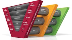
Higher-speed connections and SWaP (size, weight, and power) consistently raise the complexity level of printed-circuit-board (PCB) design. On top of that, growing system complexity often increases the number of layers used in a PCB. This requires tighter integration with other chip and system design tools, in addition to PCB design tools, to handle these constraints (Fig. 1).
In particular, as high-speed serial interfaces push the performance envelope, PCB design tools must keep pace. Differential traces for USB 3.0, PCI Express Gen 3, and 40- and 100-Gbit Ethernet are the norm these days. PCB design for PCI Express Gen 2 and 1-Gbit Ethernet seems almost trivial now.
PCBs aren’t designed in isolation. Designers need to consider chip criteria, where denser BGAs can wreak havoc on layout. The ability to change a chip layout may significantly impact the cost and reliability of the PCB, and, hence, the overall system.
Likewise, thermal and vibration issues can affect the PCB’s surrounding environment. Increased use of simulation for all aspects of design provides useful feedback to designers, but MCAD (mechanical computer-aided design) and ECAD (electrical/electronic CAD) designers often use different tools. Integrating these and other tools helps reduce turnaround time, overhead, and errors compared to manual integration of data between these tools. Spreadsheets are great, but they’re not the best way to manage and exchange engineering change orders (ECOs) between tools.
ECAD and MCAD Integration
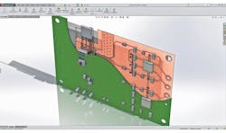
Altium's PCBWorks, which tightly integrates with Dassault Systemes SolidWorks, typifies the integration of ECAD and MCAD integration. SolidWorks is a well-known 3D MCAD tool that has extensive simulation and integration support with a range of tools, including PCBWorks.
PCBWorks, based on the Altium Designer PCB design tool for 3D board design, has migration capabilities from Designer. However, the tight integration between PCBWorks and SolidWorks requires the former to be its own platform, which would enable improvements to grow between it and SolidWorks.
This file type includes high resolution graphics and schematics when applicable.
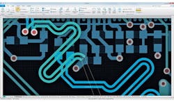
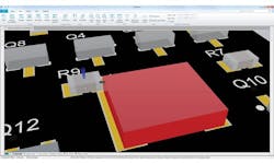
PCBWorks can handle the latest differential layouts for high-speed serial interfaces (Fig. 2). It also takes on various 3D chores, such as highlighting 3D clearance errors (Fig. 3). These are typical features for high-end PCB layout programs. The key difference here, though, is its integration with SolidWorks, which includes a bidirectional data-synch exchange at the database level for ECOs.
A typical scenario would be a SolidWorks designer dealing with a mechanical simulation and discovering that something like the mounting hold on a circuit board is causing a problem. The fix may be simply enlarging the hole or moving it slightly. Of course, this “minor” change could turn out to be significant—such a movement may require a major redesign due to the need to adjust differential-pair traces.
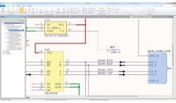
The SolidWorks change would be fed back to PCBWorks, where a designer could see the implications of the change (Fig. 4). Actual scenarios tend to be more complicated; the affect, and the amount of information that needs to be exchanged, could be substantial. This includes version control and collaboration information, which is why the system incorporates social collaboration tools. Comments may state reasons why a particular change was needed, or how it was made. Such interaction can be crucial, because alternatives are often included and changes won’t be finalized until there’s agreement among all parties.
The bidirectional exchange works both ways, with SolidWorks designers getting more, and timelier, information about a circuit board. Details could be, for instance, the copper involved in a design (Fig. 5). SolidWorks simulations will take an entire system into account, addressing a range of areas like thermal, EMI, power integrity, and mechanical vibration. PCBWorks supports SolidWorks Parasolid models, which provide detailed board-assembly support.
Another advantage of the integrated, bidirectional exchange is that there is no loss of data integrity. A simple file exchange, on the other hand, could suffer from that issue.
PCBWorks represents one example of very tight integration. It works only with SolidWorks, so companies with a vested interest in other MCAD tools will have to look at other alternatives.
PCB and Chip Design
PCB layout is performed to connect components like chips and passive devices such as resistors and capacitors. Layout of these devices dictates the overall layout, as well as the confines of the board. Low-density packages can create layout challenges, but potentially becomes a nightmare when it involves high-density ball-grid-array (BGA) packages. These can have hundreds of connections, and spacing of the BGAs has become ever-tighter.
Many high-density BGAs are custom designs in which the vendor can manipulate one or more chip designs as well as the PCB layout. Optimization may take many forms. For example, running a bus between two chips works best if the pins for the bus on each chip are aligned. Another optimization is reducing the number of layers required for BGA support. The pin out can affect how signals are moved to different layers and how they can be spread out from that point. Eliminating a layer can produce significant cost and performance benefits.
Mentor Graphics offers products that handle everything from IC design to PCB design to real-time operating systems. For example, its Xpedition Package Integrator addresses IC design integration with the PCB design. The combination works especially well with the company’s own tools, but it takes a more generic approach when working with third-party tools using industry-standard file formats. This allows for its incorporation across a wider community.
A typical scenario for the Xpedition Package Integrator would be when a user has control over the IC design, chip-package design, and PCB design. This would be the case for a company designing a chip and a reference design or a final product. The ability to change the chip’s pin out can radically affect the PCB design, leading to a lower-cost solution with higher reliability or better performance.
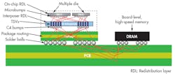
The issues become even more complex when considering today’s complex multi-die packages and multichip solutions that utilize high-speed serial links. Multichip BGAs that integrate interposers and through-silicon vias (TSVs) highlight the level of complexity for a simple chip (Fig. 6). The ability to run dozens of differential pairs between chips, or to connectors, in an efficient manner can make the difference between a viable product and something that never gets out of the lab.
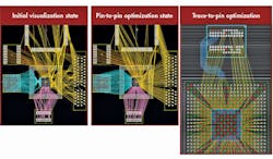
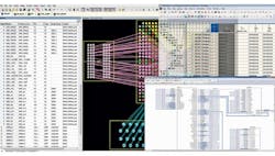
The Xpedition Package Integrator uses a virtual die model concept for true IC-to-package co-optimization. As a result, the tool is able to work with a range of other tools, not just Mentor Graphics IC design tools. It supports multimode connectivity between tools using standard hardware description language (HDL) to provide features like cross-domain pin-mapping (Fig. 7) and system-level cross-domain logical verification.
The cross-domain interconnect visualization can be presented in a single view (Fig. 8). Different presentation formats are necessary because of the range of designers that will utilize the tool. Each has a preferred view of the data, but they must be provided with the related cross-reference information. For example, the signal designation inside a chip design may differ from the pin-out name as well as the logical signal name in the PCB schematic.
Like PCBWorks, Xpedition Package Integrator is designed to provide data exchange between tools in addition to providing its own design functionality. Xpedition Package Integrator leverages tools such as HyperLynx for signal and power integrity, FloTHERM for its computational-fluid-dynamics (CFD) thermal-modeling tools, the Valor NPI substrate fabrication checking tool, and the Nimbic Maxwell-accurate, 3D full-wave electromagnetic (EM) high-performance simulation that can manage complex electromagnetic fields for chip-package-board simulation.
No single solution addresses all of the issues in system design. Nonetheless, the level of integration and cooperation between vendors has soared, with a commensurate reduction in turnaround time, overhead, and errors. Not all projects will require this level of integration, but the payback is compelling.
This file type includes high resolution graphics and schematics when applicable.
