Ceramic Packaging: When You Really Need Rugged
What you’ll learn:
- Where ceramic packaging and substrates are employed.
- Why designing solutions with ceramic packaging and substrates is challenging.
Ceramic packaging and substrates address high-performance and reliability requirements for many electronic applications, especially those found in rugged systems or where consistency and reliability are critical factors. This is particularly apparent in the RF and microwave space.
Remtec uses a proprietary technology called plated copper on thick film (PCTF). It can deliver high levels of product uniformity, yield consistency, and reliability. I talked with Remtec’s President, Brian Buyea, about the company’s offerings and the challenges and advantages of using ceramic technology in electronic devices (watch the video above).
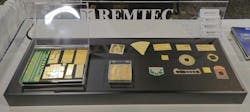
Remtec provides a range of ceramic-based solutions from circuit boards and modules (see figure) to standard TO-style, surface-mount-technology (SMT) packages. Laser and photodiode submount assemblies leverage the company’s PCTF technology with a direct-bond-copper (DBC) metallization option, too. Most of the work is customized to accommodate solutions as well as materials and chips supplied by the customer for packaging.
The company also has subject-matter experts to assist in the design of systems, including testing and quality control.
Links
About the Author
William G. Wong
Senior Content Director - Electronic Design and Microwaves & RF
I am Editor of Electronic Design focusing on embedded, software, and systems. As Senior Content Director, I also manage Microwaves & RF and I work with a great team of editors to provide engineers, programmers, developers and technical managers with interesting and useful articles and videos on a regular basis. Check out our free newsletters to see the latest content.
You can send press releases for new products for possible coverage on the website. I am also interested in receiving contributed articles for publishing on our website. Use our template and send to me along with a signed release form.
Check out my blog, AltEmbedded on Electronic Design, as well as his latest articles on this site that are listed below.
You can visit my social media via these links:
- AltEmbedded on Electronic Design
- Bill Wong on Facebook
- @AltEmbedded on Twitter
- Bill Wong on LinkedIn
I earned a Bachelor of Electrical Engineering at the Georgia Institute of Technology and a Masters in Computer Science from Rutgers University. I still do a bit of programming using everything from C and C++ to Rust and Ada/SPARK. I do a bit of PHP programming for Drupal websites. I have posted a few Drupal modules.
I still get a hand on software and electronic hardware. Some of this can be found on our Kit Close-Up video series. You can also see me on many of our TechXchange Talk videos. I am interested in a range of projects from robotics to artificial intelligence.


