Amathematical model is always helpful in determining the optimal compensation components for a particular design. However, compensating the loop of a WLED current-regulating boost converter is a bit different than compensating the same converter configured to regulate voltage. Measuring the control loop with traditional methods is cumbersome because of low impedance at the feedback (FB) pin and the lack of a top-side FB resistor. In Reference 1, Ray Ridley has presented a simplified, small-signal control-loop model for a boost converter with current-mode control. The following mathematical model explains how to modify Ridley's model so that it fits a WLED current-regulating boost converter; it also explains how to measure the boost converter's control loop.
LOOP COMPONENTS
As shown in Fig. 1, any adjustable DC/DC converter can be modified to provide a higher or lower regulated output voltage from an input voltage. In this configuration, if we assume ROUT is a purely resistive load, then V OUT = IOUT × ROUT. When used to power LEDs, a DC/DC converter actually controls the current through the LEDs by regulating the voltage across the low-side FB resistor as shown in Fig. 2. Because the load itself (the LEDs) replaces the upper FB resistor, the traditional small-signal control-loop equations no longer apply. The DC load resistance is:
REQ = VOUT/ILED
(1)
VOUT = n × VFWD + VFB
(2)
VFWD, taken either from the diodes' datasheet or from measurements, is the forward voltage at ILED; and n is the number of LEDs in the string.
However, from a small-signal standpoint, the load resistance consists of REQ as well as the dynamic resistances of the LEDs, rD, at the ILED. While some LED manufacturers provide typical values of rD at various current levels, the best way to determine rD is to extract it from the typical LED I-V curve, which all manufacturers provide. Fig. 3 shows an example I-V curve of an OSRAM LW W5SM high-power LED. Being a dynamic (or small-signal) quantity, r D is defined as the change in voltage divided by the change in current, or rD =πVFWD/πILED. To extract rD from Fig. 3, we simply drive a straight tangent line from the V FWD and ILED for the application and compute the slope. For example, using the dotted tangent line in Fig. 3, we get r D = (3.5 - 2.0 V)/(1.000 - 0.010 A) = 1.51W at ILED = 350 mA.
SMALL-SIGNAL MODEL
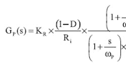
As an example of a small-signal model, the TPS61165 peak current-mode converter driving three series OSRAM LW W5SM parts will be used. Fig. 4a shows an equivalent small-signal model of a current-regulating boost converter, while Fig. 4b shows an even more simplified model. Equation 3 shows a frequency-based (s-domain) model for computing DC gain in both the current-regulating and the voltage-regulating boost converters:
where the common variables are:
and
The duty cycle, D, and the modified values for VOUT and REQ are computed the same way for both circuits. Sn and Se are the natural inductor and compensation slopes, respectively, for the boost converter; and fSW is the switching frequency. The only real differences between the small-signal model for the voltage-regulating boost converter and the model for a current-regulating boost converter is the resistance KR — which multiplies by the transconductance term, (1-D/Ri) — and the dominant pole, ωP. These differences are summarized in Table 1 [1].
Since the value of RSENSE is typically much lower than that of ROUT in a converter configured to regulate voltage, the gain for a current-regulating converter, where ROUT =REQ, will almost always be lower than the gain for a voltage-regulating converter.
MEASURING THE LOOP
To measure the control loop gain and phase of a voltage-regulating converter, a network or dedicated loop-gain/phase analyzer typically uses a 1:1 transformer to inject a small signal into the loop via a small resistance (RINJ). The analyzer then measures and compares, over frequency, the injected signal at point A to the returned signal at point R and reports the ratio in terms of amplitude difference (gain) and time delay (phase). This resistance can be inserted anywhere in the loop as long as point A has relatively much lower impedance than point R; otherwise, the injected signal will be too large and disturb the converterís operating point. As shown in Fig. 5, the high-impedance node where the FB resistors sense the output voltage at the output capacitor (low-impedance node) is the typical place for such a resistor.
In a current-regulating configuration, with the load itself being the upper FB resistor, the injection resistor cannot be inserted in series with the LEDs. The converter's operating point must first be changed so the resistor can be inserted between the FB pin and the sense resistor as shown in Fig. 6. In some cases, a non-inverting, unity-gain buffer amplifier may be necessary to lower the impedance at the injection point and reduce measurement noise.
With the measurement setup in Fig. 6 but without the amplifier, and with R INJ = 51.1W, a Venable loop analyzer was used to measure the loop. The model of a current-regulating converter was constructed in Mathcad® using the datasheet design parameters of the TPS61170, which has the same core as the TPS61165. With VIN = 5 V and ILED set to 350 mA, the model gives the predicted loop response for the TPS61165EVM as shown in Fig. 7, which provides an easy comparison with measured data.
We can easily explain the differences between the measured and simulated gain by observing variations in the WLED dynamic resistance and using the typical LED I-V curve as well as chip-to-chip variations in the IC's amplifier gain.
CONCLUSION
While not exact, the mathematical model described here gives the designer a good starting point for designing the compensation circuit for a WLED current-regulating boost converter. In addition, the designer can measure the control loop with one of the alternate methods.
REFERENCES
-
Ray Ridley. (2006). Designer's Series, Part V: Current-Mode Control Modeling. Switching Power Magazine[Online]. Available: http://www.switchingpowermagazine.com/downloads/5%20Mode%20Control%20Modeling.pdf
