For thirty-seven years after introduction of the first three-terminal adjustable linear regulators, this topology has seen virtually no major architectural changes. These older generation linear regulators limit the minimum output voltage to 1.2 V because their architecture employs a 1.2 V reference. Thus, these linear regulators cannot power ICs that require less than 1.2 V.
Now, a new linear regulator architecture eliminates this low output voltage limitation. It adapts to these lower output voltages by throwing away the voltage reference and replacing it with a current source. Linear Technology’s LT3801 uses this approach to provide the ability to approach a zero voltage regulated output. It requires only a 5 mA minimum load for proper output regulation.
The new regulator architecture allows paralleling devices to provide higher output currents. This overcomes a major problem when using older linear regulators whose peak temperature limited power dissipation to 2 W. This prevented use of only surface mount components on high density boards because of height restrictions precluded heat sinks with older linear regulators.
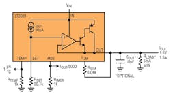
By using this new linear regulator architecture, the LT3081 provides 1.5 A for rugged industrial applications (Fig. 1). Key features of the IC are the extended safe operating area (SOA) and the ability to withstand reverse input and reverse output-to-input voltages without reverse current flow.
Included in the IC is the monitoring of die junction temperature and output current, which provide debug capability.The LT3081 delivers a current proportional to the internal average junction temperature, whose output is 1 μA/°C for temperatures above 5 °C. The output current monitor sources a current typically equal to ILOAD/5000 or 200 μA per ampere of output.
A single external resistor programs the IC’s current limit threshold level lower than the internal current limit. Tolerance over temperature is 15%, so current limit is normally set 20% above maximum load current. The internal current limit overrides the programmed current limit if the input-to-output voltage differential is excessive.
A precision 50 µA reference current source allows the LT3081 to use a single resistor to program output voltage to any level between zero and 34.5 V. And, the current reference architecture makes load regulation independent of output voltage. Plus, the LT3081 is stable with or without input and output capacitors.
This IC fits well in applications needing multiple rails. Its new architecture that adjusts down to zero allows it to handle modern low voltage digital ICs as well as allowing easy parallel operation and thermal management without heat sinks. Adjusting to zero output enables shutting off the powered circuitry.
Why do so many regulators limit the minimum output to 1.2 V? It is not until recently that digital (or any) circuit needed operation below 1.2 V. The answer is that the basic bandgap reference voltage is 1.2 V. The simplest bandgap reference had an inherent reference voltage of 1.2 V. This type of bandgap uses a positive coefficient voltage in series with a single emitter-base voltage. It is stable, easy to set up and can be stacked for high voltage. But it needs to be divided down for lower voltage. Dividing down adds uncertainty in the reference voltage and requires higher gain amplifiers for higher outputs so it was not needed until recently. A trimmed current source reference overcomes these problems.
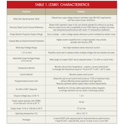
Table 1 summarizes characteristics of the LT3801.


