Charge Pump DC/DC Controller IC Eliminates Magnetics, Configures Bus Converter
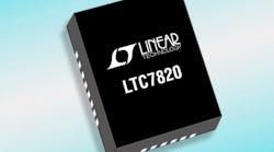
Linear Technology’s LTC7820 is a high-power fixed-ratio charge pump dc/dc controller IC that eliminates the need for any magnetic component in a non-isolated intermediate bus converter (IBC). This provides up to a 50% reduction in circuit size and up to 4000W/in.3 power density (Fig. 1). Additional features include soft switching for low EMI, a “power good” output signal, undervoltage lockout, and internal charge balance circuitry. The LTC7820 is available in a 4mm × 5mm QFN-28 package. Extended and industrial temperature versions are available from –40 to 125°C.
1. LTC7820 Charge Pump DC/DC Controller.
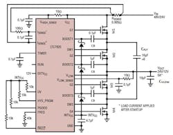
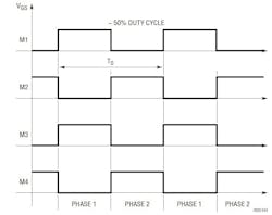
The LTC7820 employs four external power MOSFETS, as shown in Fig. 1. The N-channel MOSFETs M1 and M3 are turned on and off in the same phase with around 50% duty cycle at a pre-programmed switching frequency. The N-channel MOSFETs M2 and M4 are turned on and off complementarily to MOSFETs M1 and M3. During phase 1, M1 and M3 are on and the flying capacitor, CFLY, is in series with CVLOW. During phase 2, M2 and M4 are on and CFLY is in parallel with CVLOW . The VLOW pin voltage is always close to half of the top voltage at the drain of MOSFET M1 (refer to GND pin) in steady state, and it is not sensitive to variable loads due to the very low impedance at its output. Figure 2 shows the timing diagram for switching M1, M2, M3, and M4.
2. Timing diagram for switching M1, M2, M3, and M4 power MOSFETs.
The IC does not regulate the output voltage with a closed-loop feedback system. However, it stops switching when fault conditions occur, such as VLOW pin voltage overvoltage or undervoltage, an overcurrent event or an overtemperature protection event.
This IC operates over a 6V to 72V (80V max.) input voltage range and can produce output currents in the 10s of amps, depending on the topology and choice of external components. You can configure the LTC7820 for:
- 2:1 step-down ratio for VIN up to 72V
- 1:2 step-up ratio for VINUp to 36V
- 1: –1 ratio as an inverter from VIN up to 36V
In addition, you can cascade two LTC7820s for a 4:1 step-down ratio. For even higher step-down ratios, such as a 6:1, the Dickson converter topology is recommended and is ideal for 54V input to a 9V outputs, requiring only a single LTC7820. External MOSFETs switch at a fixed frequency, programmable from 100kHz to 1MHz. The LTC7820’s 1.1Ω N-channel MOSFET gate drivers maximize efficiency and can drive multiple MOSFETs in parallel for higher power applications.
Power MOSFETs and Schottky Diodes
The four internal MOSFET gate drivers are powered by INTVCC, Schottky diodes forward voltage drop and switching frequency. The lowest driver voltage is the top MOSFET (M1) drive voltage running at high switching frequency and cold temperature. It is normally around 4.2V so logic-level threshold MOSFETs must be used in most applications. Threshold voltage of some logic-level MOSFETs varies with temperature. If switching frequency is high and temperature range is wide for specific applications, the top driver voltage of MOSFET M1 may be as low as 4V, and sub-logic level threshold MOSFETs (VGS(TH) < 3V) should be used.
Selection criteria for the power MOSFETs includes the on-resistance RDS(ON), output capacitance COSS, input voltage, and maximum output current. Generally, low RDS(ON) and low COSS MOSFETs are preferred in switched capacitor applications because they minimize both conduction and switching losses.
For a given input and output voltage, the uppermost MOSFET M1 always sees high voltage during startup and shutdown. The drain-to-source voltage of M1 has to be high enough to survive at full input voltage range. Other MOSFETs normally only see half of the input voltage, so the breakdown voltage of M2/M3/M4 can be lower than M1 to optimize RDS(ON) and COSS. If the reliability of M1 is a major concern, the same high-voltage MOSFETs could also be used as M2/M3/M4 to protect against M1 short conditions.
External Schottky diodes are needed for the bootstrap circuits, and provide voltage for the floating drivers. To minimize the voltage drop on the top gate driver, low forward voltage drop Schottky diodes are preferred with load current in the 10mA to 50mA range. The reverse breakdown voltage of the diodes should be high enough to survive at the maximum operation voltage between the VLOW and GND pins.
Faults
The LTC7820 monitors system voltage, current and temperature for fault protection. It stops switching and pulls the FAULT* pin low when a fault condition occurs. You can set an onboard timer for appropriate restart/retry times. The EXTVCC pin permits the LTC7820 to be powered from the lower voltage output of the converter or other available sources up to 40V, reducing power dissipation and improving efficiency.
For overcurrent protection, the LTC7820 uses sense resistor, RSENSE, to monitor input current. Place the sensing resistor at the drain of the very top MOSFET, M1. For voltage divider and inverter applications, the current flows into the drain of the MOSFET M1, so the ISENSE + pin should be connected to the sensing resistor then to the drain of the MOSFET M1. For voltage doubler applications, the current flows out of the drain of the MOSFET M1, so the ISENSE + pin should be connected directly to the drain of the MOSFET M1. In most applications, the current through the sense resistor is a pulse current and the peak value is much higher than the average load current. A RC filter on the ISENSE – pin, with a time constant lower than the switching frequency, may be used to set the precision average current protection. If overcurrent protection is not desired, short the ISENSE + and ISENSE– pins together and connect them to the drain of the top MOSFET M1 directly.
To clear voltage faults, the LOW_SENSE pin voltage has to be within the programmed window around half of HIGH_SENSE voltage or the VHIGH_SENSE and VLOW_SENSE voltages must be lower than 1V and 0.5V respectively. To clear the current fault, the voltage drop from ISENSE + pin to ISENSE – pin has to be lower than 50mV. To clear temperature faults, the IC temperature has to be lower than 165°C. The FAULT* pin may be pulled up by external resistors to voltages up to 80V. It can be used to control an external disconnect FET to isolate the input and output during fault conditions.
Gate Driver Power
Power for the four MOSFET drivers and most other internal circuitry is derived from the INTVCC pin. Normally, an internal 5.5V linear regulator supplies INTVCC power from VCC. If VCC is connected to a high input voltage, an optional external voltage source on the EXTVCC pin enables a second 5.5V linear regulator and supplies INTVCC power from the EXTVCC pin. To enable this more efficient second regulator, VCC needs to be higher than 7V and the EXTVCC pin voltage has to be higher than 6.5V. Do not exceed 40V on the EXTVCC pin. Each top MOSFET driver is biased from the floating bootstrap capacitors, CB, which are normally recharged during each off cycle through an external Schottky diode when the respective top MOSFET turns off.
Startup and Shutdown
Putting the RUN pin lower than 1.14V shuts down the LTC7820. In this mode, most internal circuitry is turned off including the INTVCC regulator and the LTC7820 consumes less than 100μA. All gates G1/G2/G3/G4 are actively pulled low to turn off the external power MOSFETs in shutdown. Releasing RUN allows an internal 1μA current to pull up this pin and enable the controller.
Once the RUN pin rises above 1.22V, an additional 5μA flows out of this pin. As an alternative, the RUN pin may be externally pulled up or driven directly by logic. Do not exceed the absolute maximum rating of 6V on this pin. After the RUN pin is released and the INTVCC voltage passes UVLO, the LTC7820 starts up and monitors the VHIGH_SENSE and VLOW_SENSE voltages continuously. The LTC7820 starts switching only if VLOW_SENSE voltage is close to half of VHIGH_SENSE voltage or both VLOW_SENSE and VHIGH_SENSE voltages are close to GND. In voltage divider applications, VLOW is pre-balanced to half the VHIGH_SENSE voltage and the LTC7820 may start up with capacitors at different initial conditions.
Selection of switching frequency is a trade-off between efficiency and component size. Low frequency operation increases efficiency by reducing MOSFET switching losses, but requires larger capacitance to maintain low output ripple voltage and low output impedance. The FREQ pin can be used to program the controller’s operating frequency from 100kHz to 1MHz with a single resistor to GND.
Power Good
When the UV (undervoltage) pin voltage is lower than 1V, the PGOOD pin is pulled low. The PGOOD pin is also pulled low when the RUN pin is low or when the LTC7820 is starting up. The PGOOD pin is released only when the LTC7820 is switching and UV pin is higher than 1V. The PGOOD pin will flag “power bad” immediately when the UV pin is low. However, there is an internal 20μs power-good mask and 100mV hysteresis when UV goes higher than 1V. The PGOOD pin may be pulled up by external resistors to sources up to 45V.
PGOOD signal can be used to enable or disable the output loads. If the loads are switching mode converters or LDOs with ENABLE/RUN pins, this allows easy interfacing. With proper setup on the UV pin, PGOOD can enable the loads at the output when the output voltage is above a certain value. PGOOD can also be used to control the RUN pin of another LTC7820 if two or more parts are cascaded to achieve higher step-down ratios.


