Smart Power Technology Requires Smart Isolated Substrates
The semiconductor substrate is the foundation of high-technology products, the simplest being the silicon wafer. However, to meet new technical challenges, intelligent substrates such as silicon-on-insulator (SOI) are used for making specific types of digital or analog ICs. An example is the SOI substrate for radio-frequency (RF-SOI) applications to provide the necessary connectivity performance for mobile phones. Another is the fully depleted SOI (FD-SOI) to enable ultra-low-power consumption in microprocessor chips. These smart substrates address the new technological challenges facing the design of electronic systems.
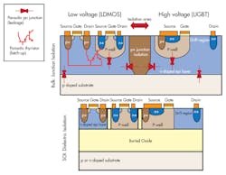
Smart power applications also benefit from SOI substrates. They provide the ability to isolate mixed signal semiconductors that operate at different voltages, so they must be electrically isolated from each other. Isolation is required between: CMOS used for logic, DMOS for high voltage, and bipolar for analog functions. You can obtain this isolation by two main techniques as shown in Fig. 1:
· Junction isolation: P-N junctions are inserted between the blocks to prevent current flow
· Oxide isolation: oxide trenches and an SOI substrate are used to fully isolate the blocks
The junction isolation technique consists of adding an additional doped area in between voltage blocks to allow the formation of a blocking P-N junction preventing any current flow. To be effective, the implantation depth and width must be large enough to block the voltage difference and must increase with the voltage difference—on the order of 15µm width for 40V (low voltage) and up to 100µm or more for 600V (high voltage). Subsequently, die size increases with multiple voltage domains and increases very quickly with higher voltage applications.
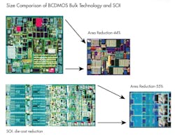
The oxide isolation technique uses an existing oxide layer pre-embedded into the substrate (called buried oxide or BOX) to provide electrical isolation between the substrate and the device layer. The resulting wafer is called SOI. To complete the electric isolation, a trench through the top silicon thickness is inserted down to the BOX to form a fully dielectrically isolated silicon island on the substrate. The trench width is typically on the order of 1.6µm (Atmel2), which is from 6 times to 40 times smaller than junction isolation depending of the maximum targeted voltage. The use of SOI-based BCDMOS technology results in a smaller die size compared to the bulk equivalent design using junction isolation, as has been demonstrated by Atmel3 (Fig. 2). This size reduction or die shrink depends on the number of power functions implemented on the die as well as the maximum voltage those functions must handle. The higher the power and maximum voltage, the greater the die shrink.
Besides die size reduction, the presence of a BOX layer enables several other benefits. Because the devices are fully dielectrically isolated, they can operate at different potentials, which greatly simplifies integration. And because oxide isolation can support higher voltage, the integration of an insulated gate bipolar transistor (IGBT) becomes an option; this is not possible with junction isolation.4 This presents an enormous design advantage for high- and low-voltage integration as the different areas can be independently biased. It also allows positive and negative voltage supplies to be integrated on the same chip.
Additional Benefits
SOI also enables design simplification and performance enhancement. Thanks to dielectric isolation between blocks, there is no current flow possible through the substrate between adjacent transistors. As a result, latch-up caused by parasitic thyristor (PNPN junction) cannot happen5 (Fig. 1). This simplifies protection schemes and chip design, providing further die size reduction and shorter time-to-market benefits.
Furthermore, because dielectric isolation replaces many pn-junctions, the effective parasitic capacities and PN junctions are smaller. Current leakage is reduced by a factor of 50, especially at high temperature.6 It also improves the switching speed of the SOI-LIGBT devices to a turn-off speed of 0.8µs, down from approximately 10µs for the junction isolation equivalent.7
Because parasitic effects are difficult to model, their reduction limits the design reliance on empirical models. Thanks to robust isolation between blocks, designing right the first time is easier to achieve, providing a real time-to-market advantage.
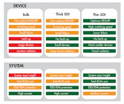
To summarize these benefits, we have grouped the transistor performance enhancement into five categories related to die performance: high-temperature operation, high reliability, high performance, integration and high voltage. Figure 3 highlights these benefits.
Design with SOI
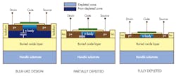
There are three main techniques for BCDMOS transistor design with SOI: bulk-like approach, partially depleted SOI and fully depleted SOI, as described in Fig. 4.
Bulk-like transistor design is implemented on a thick SOI layer (more than 5µm up to several tens of microns) and the source and drain structures are doped on the first few microns at the surface of the layer in the same manner as a bulk design. It enables a robust high-voltage and high-current transistor design. The main drawback is that the large remaining parasitic capacitance below the source and drain increases leakage current and limits the switching frequency. At the system level in a power converter, for example, it impacts standby power consumption as well as power-conversion efficiency.
Partially and fully depleted designs are realized on a thin top SOI layer (partially depleted is ~1µm and fully depleted is <1µm) and therefore the source and drain implantation reaches the BOX layer.8 A smaller PN junction area greatly reduces the parasitic capacitor and leakage current.
In addition to pure device-level benefits, SOI-BCDMOS technology improvements also translate into advantages at the design and system levels.[9] The devices exhibit higher reliability, especially at high temperature, making them suitable for automotive and industrial applications in harsh environments. It also enables system-level board simplification, a shorter Bill of Materials (BOM), smaller form factors and reduced PCB sizes because the final die size is smaller and the number of external elements is reduced.
Figure 5 provides a comparative summary of the benefits between bulk, thin SOI, and thick SOI-based devices and systems.
As a result, many industry players have adopted this technology and are currently using it in several applications such as automotive, lighting, plasma panel drivers, AMOLED displays, power over Ethernet and ultrasound medical systems. Attracted by the benefits this technology has to offer, most power semiconductor companies have developed an SOI-BCDMOS platform. These companies include NXP, Atmel, STMicroelectronics, Renesas, Freescale, Infineon, T.I., AMS, X-FAB and other power IC players. Commercial products have been introduced since the early 2000s and are now in mass production.
We also see foundries offering SOI options on their power-management process because it enables them to propose higher supported voltage. This offering opens the door for fabless semiconductor companies to design devices targeted at higher power applications using a SOI-BCDMOS platform.10
SOI Products
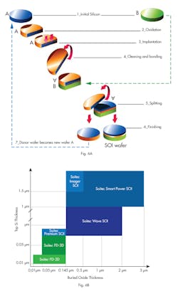
SOI substrates are included in a comprehensive Soitec product line that covers all smart power BCDMOS needs. Figure 6 shows both the conceptual method of creating Soitec’s SOI products and a high-level overview of its product portfolio. This Smart Power SOI family has been specially designed for BCDMOS platforms and is widely used throughout the industry.
The Smart Cut technology used to produce SOI wafers provides several advantages compared to other technologies (wafer bonding and grinding, SIMOX and seed methods):
· Low cost thanks to the multiple reuse of the top wafer
· Thermal oxide quality with sharp transition between silicon and oxide
· Excellent across-wafer and wafer-to-wafer uniformity of the silicon layer
· Excellent doping level uniformity
This Smart Power SOI product line therefore offers customers the following benefits:
· SOI high-volume and low-cost wafer supply
· High breakdown voltage
· Reduced design margin to reduce die size
· Partially or fully depleted design options.
References
1. http://www.iue.tuwien.ac.at/phd/triebl/node10.html
3. http://www.atmel.com/Images/atmel_autocompilation_vol4_oct2007.pdf
4. Eric Cirot and Pierre Fournier, Use high-voltage drivers for large flat-panel displays. Electronic Engineering Times-Asia, November 16-30, 2006
5. http://am.renesas.com/company_info/magazine/2004/vol_0019/index.jsp
6. http://www.bdtic.com/DownLoad/ATMEL/Semiconductor/Atmel_Motor_Driver_Solutions.pdf
7. D. M. Garner and al., Silicon-on-insulator power integrated circuits, Microelectronics Journal, pp. 517-526, 2001
8. http://www.xfab.com/en/about-x-fab/events/webinar-overview, Gabriel Kittler and Sebastian Schmidt, Benefits and Trade-offs of SOI Designs for Applications up to 200V. XFAB webinar, 2012
9. Piet Wessels, Power Devices on SOI. MIGAS 2009
10. TowerJazz and TPSCo Release Enhanced up to 200V 180nm BCD on SOI Power Management Process - https://tpsemico.com/2017/03/200v-bcd-on-soi/

