Implementing Synchronous Rectification in Non-Isolated DC-DC Converters
This article discusses the implementation of synchronous rectification in non-isolated DC-DC converters. The article explains the advantages along with some of the extra considerations needed in circuit design to achieve the best performance from the technique.
Quality OFF Time
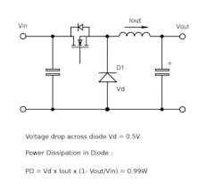
The most basic diagrams depicting non-isolated DC-DC converters generally show two ideal switches and an energy storage inductor. In early designs, it was quickly realized that one switch could be replaced by a low-cost diode; it turned itself on naturally at the right instant by ‘commutation,’ the action of the inductor reversing its voltage during the main switch OFF time and forward-biasing the ‘free-wheeling’ diode D1 (Figure 1).
This is great for simplicity and although the diode does drop some voltage while it is circulating output current, this represents little percentage power loss when the output voltage is relatively high.
Over the years, however, output voltages have plummeted to below 1V for processors and other ICs to increase operating speed while maintaining low dissipation. Ironically, this just pushes the efficiency problem back to the DC-DC converter power source as now the diode voltage drop becomes a much larger proportion of the output voltage. A 1V diode drop with a 1V output will dissipate the same amount of power that the converter is delivering to the load during the OFF time (1-D). This means the converter has approximately only 50% efficiency during this period. The impact of this low efficiency to the overall converter efficiency depends on the input/output voltage ratio and the efficiency during the ON time. Higher DC-DC input-output voltage differentials make the problem worse with the associated longer OFF times.
The Ideal Switch
The solution has been to try to get back to the ideal switch for SW2 with minimal voltage drop and, although bi-polar transistors were originally tried, a MOSFET is the obvious choice. Initially they were limited to lower current applications as their losses are proportional to current squared, whereas diodes were simply proportional. But, nowadays, RDS(on) values are so low that high current applications are viable as well. MOSFET total gate charge values (Qg) have also dropped, significantly reducing drive losses and enabling higher operating frequencies. Another benefit is that MOSFETs can be paralleled as discrete devices or multiple die in ICs, giving more than proportionally better performance with lower net ON resistance and lower die temperatures. They have a positive temperature coefficient for RDS(on) so naturally share current, unlike diodes which can be paralleled but without guaranteed current sharing. A MOSFET, of course, has to be actively driven on and off but simply in direct antiphase to the main switch with a ground referenced signal, which is easy to integrate into control ICs. It is vital that the two switches are not on together, even momentarily, as this would be a direct short across the input supply with potential damage to semiconductors and PCB traces.
In practice, a ‘dead-time’ between ON periods of the switches is imposed by the control IC to guarantee no ‘shoot-through.’ During the dead time, commutation still happens with the intrinsic body diode of the MOSFET. This diode usually has a relatively high forward voltage drop and long reverse recovery time, so it can produce significant dissipation if the dead time is allowed to be too long. However, tight control of timing within the control IC minimizes these problems. Another work-around is to fit a Schottky diode in parallel with the MOSFET so it conducts before the body diode, but this adds cost to the solution.
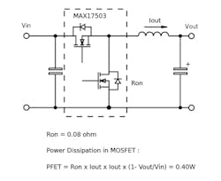
A simple comparative example is given in Figure 1. Here, power losses in a DC-DC converter producing 5V/2.5A from 24V are compared using a diode and synchronous rectifier. Even with 5V out, the advantages are clear; losses are more than halved from 0.99W to 0.4W in the rectifier. Even if a Schottky diode is used, the gain is still significant. With lower output voltages the improvement is more dramatic still. The result is that the lower dissipation synchronous rectifier MOSFET can now be integrated into a control IC such as the MAX17503 with lower overall converter temperature rise, 30°C in this example. Alternatively, for the same temperature rise, a smaller solution is possible.
Pre-Biased Loads
Something to watch out for is that unlike a diode, a synchronous rectifier MOSFET can conduct in both directions when turned on. In normal operation, this is not a problem. However, consider the scenario where the load requires multiple sequenced voltage rails and our DC-DC converter has to turn on last when there is already some voltage on the load, perhaps coming through a ‘sneak’ path. DC-DC converters will normally have a soft start where the duty cycle ramps up to its operating point after power-up. This means initial short ON pulses and long OFF times when the synchronous MOSFET conducts. The pre-biased load initially has a higher voltage than the DC-DC output, so current flows back into the DC-DC converter and MOSFET, perhaps preventing the DC-DC controller from starting up correctly.
The fix for this is to disable synchronous rectification during the start-up phase with the MOSFET’s body diode forming the ‘free-wheel’ diode function. Again, this is easily incorporated into control IC functionality. The extra dissipation during start-up is insignificant.
Modes of Operation
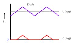
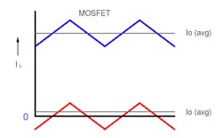
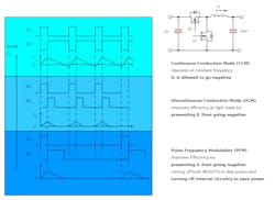
The ability of the MOSFET to conduct in both directions also has an effect on light-load operation, which can be beneficial. Looking at inductor current in Figure 2, at higher loads (upper traces), you see the familiar shape of an average DC current Io(avg) and a ripple current whose peak-to-peak amplitude is set by the inductor value and duty cycle. As the load goes to lower values (lower traces), the valley of the ripple current touches zero at the point where the load is half the peak-to-peak value of the ripple current. As the load decreases further, with diode rectification, the current stops until some point after the next on-period commences, where the current rises above zero. This is ‘discontinuous conduction mode’ (DCM). For a MOSFET synchronous rectifier, current can flow in both directions, thus remaining in ‘continuous conduction mode’ (CCM).
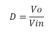
The DC-DC converter can continue to supply power and regulate in DCM, but the transfer function changes. A loop optimized for bandwidth and transient performance in CCM will generally be sub-optimal in DCM with sluggish response. In CCM, the output voltage is simply related to duty cycle D by:
For a buck converter operating in DCM, the situation is far more complex where:
You can see that the duty cycle now changes in proportion to the square root of load current, providing a more complex transfer function for the converter power stage. D also now depends on actual inductance, L, and switching frequency, Fsw. Remaining in CCM with synchronous rectification is clearly better for performance considerations. In fact, modern buck converter designs deliberately allow high ripple current values given that loop performance will not be an issue, allowing smaller values of inductors with benefits in cost and large-signal slew rate ability.
If light load efficiency is a design constraint, it can actually be better to allow discontinuous mode operation by disabling the synchronous rectifier and losing the switching and negative current conduction losses in the MOSFET. Control ICs can provide this option and others as well; for example, the IC can force a ‘pulse skipping’ mode at light loads where the ON time is kept constant. In this mode, known as ‘pulse frequency modulation’ (PFM), regulation is achieved by effectively varying the switching frequency at light load so that just sufficient energy is passed to the output to keep the voltage constant. Switching losses are proportional to frequency, so at light load these are reduced, gate drive power goes down and, as both switches can be off for long periods, some circuitry internal to the IC can be disabled for the duration, saving yet more power.
Figure 3 shows the waveforms in the various modes.
Boost Converters
Using synchronous rectification with boost and buck-boost converters is not quite so straightforward. The rectifier does not have a grounded terminal so the MOSFET drive would not be ground referenced. Perhaps more problematic is that in DCM, the control IC isn’t necessarily ‘aware’ that the stored energy has all been transferred. When this occurs at some light load before the end of the switching cycle, a diode would simply stop conducting, but a MOSFET would start conducting in reverse. In a boost converter, this would connect the output back to the input, ‘draining’ the output capacitor and dropping the output voltage. Schemes to avoid this are possible by forcing CCM with variable frequency modes or even detecting the reverse current flow through the MOSFET and cutting its drive. The issue is not significant, though, as boost converters are by definition producing higher voltages where the benefits of synchronous rectification are less important.
Synchronous rectifiers can also be used in the isolated versions of buck and boost converters where you have a choice of simple self-driven circuits or more complex but controlled versions where the drive signals cross the isolation barrier. To learn more about this subject, watch this Synchronous Switching Regulators video by Bob Mammano, the father of the first switch-mode power supply. This segment is part of a series of power system design videos which take viewers through various aspects of power-switching technology.
