Best Practices, Part 1: Integrating eGaN FETs
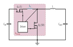
As GaN transistor switching charges continue to decrease, system parasitics must also be reduced to achieve maximum switching speeds and minimize parasitic ringing typical of power converters. In a buck converter, there are two major parasitic inductances that have a significant impact on converter performance as shown in Fig. 1.1 The common source inductance, LS, is the inductance shared by the drain-to-source power current path and gate driver loop. The high-frequency power loop inductance, LLoop, is the result of the non-zero power commutation loop area, and is comprised of the parasitic inductance from the positive terminal of the input capacitance, through the top device (Q1/T), synchronous rectifier (Q2/SR), ground loop, and input capacitor (CIN).
Where:
LS = Common Source Inductance
LLoop = High Frequency Power Loop Inductance
1. Synchronous buck converter with parasitic inductances.
It has been previously demonstrated that the chip-scale packaging of high-voltage lateral eGaN FETs have extraordinarily small parasitic inductance and resistance when compared to the Si MOSFET.2 With the lower package parasitics inherent in eGaN FET packaging, the printed circuit board layout can become the limiting factor in converter performance.
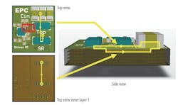
To minimize the common source inductance added by PCB layout, it is recommended that the gate driver loop and high-frequency power loop will be located where they have very little interaction. An example layout is shown in Fig. 3.2, where the gate drive loop, shown in red, and the high-frequency loop, shown in yellow, interact only directly next to the eGaN FET. This layout minimizes the common source inductance to the ultra-low internal eGaN FET package
To reduce the high-frequency power loop inductance contributed by the PCB, an optimal layout was developed that utilizes the first inner layer,1 shown in the bottom left of Fig. 2, as a high-frequency power loop return path. Located between the two eGaN FETs is a series of vias, used to connect the top layer to the inner layer return path, and arranged to match the land grid array fingers of the synchronous rectifier (Q2). This return path is located directly underneath the top layer’s power loop path, shown in the upper left of Fig. 2, allowing for the smallest physical loop size and providing magnetic field self-cancellation. The side view, as shown in Fig. 2, illustrates the concept of creating a low profile magnetic field self-cancelling loop in a multilayer PCB structure. Additional source vias are used on the lower side of the bottom transistor (Q2) to further reduce low-frequency resistance and thermal resistance.
2. PCB layout for optimal power loop with GaN transistors: top view, top view of inner layer 1, and side view.
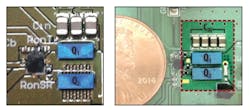
For the latest eGaN FET PCB designs,3 with an example shown on the right in Fig. 3, the vias to the inner layer return path, which were previously located outside of the device, as shown on the left of Fig. 3, have been filled and placed underneath the device. This minimizes the space between the die and further reduces the high-frequency parasitic loop inductance to approximately 250 pH, as compared to a previously reported value of 400 pH.2
The high-frequency parasitic loop inductances were experimentally measured by using the resonant frequency of the ringing voltage after the top switch (Q1) turns on. When the top switch turns on, the parasitic high-frequency loop inductance and output capacitance of the synchronous rectifier (Q2) ring at the resonant frequency, yielding:
Where:
LLoop = High-frequency loop inductance
TRing = Ringing period
COSS = Output capacitance of the synchronous rectifier at the bus voltage, where it has a nearly constant value.
3. Implementation of optimal layout without (left) and with (right) filled vias underneath the eGaN FETs.
With the introduction of eGaN monolithic half-bridges ICs,4 the parasitic inductances can be further reduced. In Fig. 4, a top view pin-out configuration of the asymmetric eGaN monolithic half-bridge IC is shown. Gate 1 is the high-side (Q1) gate pin. GR1 is the high-side gate return pin. Gate 2 is the low-side (Q2) gate pin. VSW is the switch node of the half bridge and consists of 35 solder bumps. VIN is the input voltage supplied to the drain of the top FET (Q1), and consists of eight (8) solder bumps. PGND is the power ground connection at the source terminal of the lower FET (Q2) and has 29 solder bumps.
4. Top view pin-out configuration for the asymmetric eGaN monolithic half-bridge IC (left) and asymmetric eGaN monolithic half-bridge IC demonstration board3 (right).
By integrating the two power FETs into a single monolithic device, the space needed on the PCB, as shown on the right in Fig. 4, is significantly reduced when compared to a discrete eGaN FET based design. The experimentally measured high-frequency loop inductances of the eGaN monolithic half-bridge IC, with filled vias underneath the device, is measured to be approximately 150 pH.5
Thermal Management
To estimate the thermal performance of a device, the junction temperature (TJ) can be modeled by a voltage as shown in Fig. 5.6–9 The system thermal impedances can be modeled with resistors, with junction-to-board (RθJB) and junction-to-case thermal resistances being determined by the device package and case-to-ambient (RθCA) and board-to-ambient (RθBA) thermal impedances determined by system design. A current source models power loss (PLOSS) and a voltage source models the ambient temperature (TA). The thermal resistance model is shown in Fig. 5 and can be simplified into a single resistor modeling the effective junction-to-ambient thermal impedance (RθJA) for the system and the maximum power dissipation (PMAX) of the device can be defined as:
Where:
TJMAX = Maximum junction temperature of the power device.
5. Thermal resistance model.
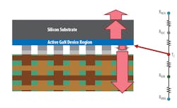
Looking at the individual thermal impedances, as illustrated in Fig. 6, it can be seen that the transistor determines the junction-to-board and junction-to-case thermal impedances. The transistor-dependent thermal impedances of eGaN FETs provide much lower thermal impedances than state-of-the-art Si MOSFETs.
The case-to-ambient and board-to-ambient impedances are greatly influenced by a variety of outside factors, such as heat sinking and PCB design. These thermal parameters vary based on air speed, heat sink sizing and attachment method, copper weight of the PCB, number and location of PCB vias, how densely the board is populated with other heat generating circuits, as well as many other design factors outside of the power device.
Silicon Substrate
6. Side view of GaN transistor mounted to a printed circuit board and thermal impedances.
Heat Sinking eGaN FETs
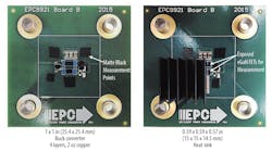
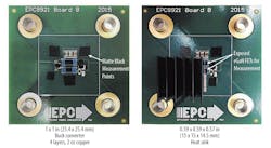
To quantify the thermal performance of eGaN FETs, a series of thermal evaluation boards were developed. The first is shown on the left of Fig. 7. Matte black thermal measurement points have been added to each board to ensure consistent emissivity for improved measurement accuracy. The thermal evaluation boards have a 1 in. by 1 in. (25.4 mm by 25.4 mm) sized area for copper, outlined in white, and a total size of 2 in. × 2 in. (50.8 mm × 50.8 mm) with the copper connections outside of the 1 in. × 1 in. (25.4 mm × 25.4 mm) white border minimized to the input and output power connection points. The circuits are configured as buck converters and the output filter inductor and output capacitors are located on the backside of the board. To evaluate the double-sided cooling benefits of eGaN FETs, a heat sink was added to the test circuit, as shown on the right in Fig. 7.
The matte black measurement points were moved to the edge of the eGaN FET die, which were left exposed, and outside of the heat sink. While locating the heat sink with a portion of the eGaN FETs exposed was not the best for thermal performance, it allowed for an accurate look at the impact of a heat sink on thermal performance. In an actual design, the heat sink should fully cover all devices to maximize heat transfer. The heat sink used in this evaluation was a 0.59 in. × 0.59 in. x 0.57 in. (15 mm × 15 mm × 14.5 mm) Advanced Thermal Solutions ATS-54150K-C2-R0, with the thermal interface material removed.
7. Thermal evaluation boards setup for cases without (left) and with (right) a heat sink.
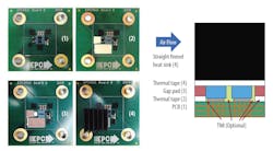
After thermal analysis was completed for a design without a heat sink, following the steps below, a heat sink (as shown in Fig. 8) was selected and attached for thermal evaluation:
- Started with the thermal evaluation board without a heat sink
- The matte black thermal measurement points from areas where the heat sink will be
- placed were removed. For the eGaN FETs, new thermal measurement points toward the end of the eGaN FET, outside of where the heat sink will be located, were added. A layer of thermal tape (3M 8810) was then added outside of the devices and inside of the 1 in. × 1 in. (25.4 mm × 25.4 mm) board area. The main purpose of the thermal tape was to act as a spacer to ensure the heat sink remains level across the small eGaN FET devices.
- A layer of gap pad (t-global TG6050) was attached on top of the thermal tape, acting as a spacer. The total height of the thermal tape with gap pad is approximately equal to the height of the eGaN FETs. It should be noted that the thermal tape and gap pad were cut to custom fit each design. A layer of thermal tape was also added to the driver to have an approximately uniform height for the heat sink.
- A heat sink was added (Advanced Thermal Solutions ATS-54150K-C2-R0 with the thermal interface material removed). The heat sink has a layer of thermal tape (3M 8810) on the bottom to assure good adhesion to the devices and provide electrical isolation. No additional pressure was applied to the heat sink in this evaluation and by using a heat sink with additional force; a further improvement in double-sided cooling capability could be realized. With additional thermal interface materials (TIM), such as thermal grease, applied between and on the sides of the devices the thermal performance could also be further improved. The use of additional TIMs was not considered in this thermal example.
8. Heat sink attachment process.
While the heat sinking in this example is minimal, the objective was to demonstrate the significant thermal performance improvements possible with eGaN FETs under a minimal heat sinking setup and to allow for easy measurement points to accurately characterize the thermal performance of an eGaN FET based design.
Measured Thermal Impedances
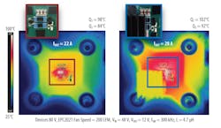
The eGaN FET thermal evaluation boards, meant to accurately represent in-circuit operating conditions, were tested as buck converters with an input voltage of 48 V, an output voltage of 12 V, and a switching frequency of 300 kHz. For the first test case, 80 V EPC2021 eGaN FETs were used.4 The circuit board for each test case is shown in the upper left and corresponding thermal images are shown in Fig. 9.
With a 200 LFM airflow, the eGaN FET design achieved an output current of 22 A before reaching a temperature around 100°C at an ambient temperature of approximately 25°C. The selected maximum temperature point for this evaluation was well below the 150°C maximum junction temperature of eGaN FETs. The 100°C point was selected to provide margin for higher ambient temperatures and provide device de-rating, which is common design practice.
When a heat sink was added to the eGaN FET based design, the output power increased by around 30% while approximately maintaining the same maximum temperature. The heat sink showed a significant temperature rise over ambient, demonstrating that the eGaN FETs were effectively moving heat from the device to the heat sink, allowing for higher output currents and power. This was enabled by the superior backside cooling properties of the eGaN FETs chip-scale packaging.
9. Thermal evaluation of eGaN FETs without (left) and with (right) a heat sink in a buck converter.
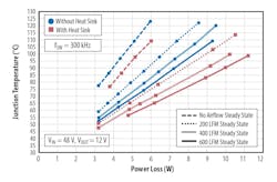
To create a more complete in-circuit thermal model of the eGaN FET based designs, the thermal evaluation boards were tested at a variety of operating points with various levels of airflow, under two test conditions, with and without a heat sink. A plot of maximum junction temperature versus total system power loss is shown in Fig. 10. The slope of these lines is equivalent to the junction-to-ambient resistance of the system, as shown in the simplified thermal schematic shown on the right of Fig. 5.
10. Plot of junction temperature vs. system power loss for a buck converter.
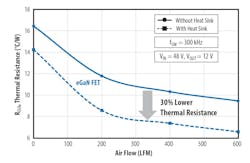
From the data in Fig. 10, the junction-to-ambient resistances are determined and plotted versus airflow in Fig. 11. It can be seen that by adding even a small amount of airflow, the thermal performance of eGaN FETs improved significantly. Also, by adding a minimal amount of heat sinking, the thermal impedance of the system decreased by around 30%. With 600 LFM of airflow and a heat sink, the effective system junction-to-ambient resistance is measured to be around 6.5°C/W, which equates to a temperature rise of 65°C for 10 watts of system power loss.
11. Plot of junction-to-ambient system thermal impedance vs. airflow for a buck converter.
References
- D. Reusch and J. Strydom, “Understanding the Effect of PCB Layout on Circuit Performance in a High-frequency Gallium Nitride Based Point-of-Load Converter,” Applied Power Electronics Conference and Exposition (APEC), pp. 649-655, 2013.
- D. Reusch, D. Gilham, Y. Su, and F. C. Lee, “Gallium Nitride Based 3D Integrated Non-Isolated Point-of-Load Module,” Applied Power Electronics Conference and Exposition (APEC), pp. 38-45, 2012.
- Efficient Power Conversion Corporation, “EPC demonstration boards.”
- Efficient Power Conversion Corporation, “EPC eGaN FETs.”
- D. Reusch, J. Strydom, and A. Lidow, “Monolithic Integration of GaN Transistors for Higher Efficiency and Power Density in DC-DC Converters,” International Exhibition and Conference for Power Electronics, Intelligent Motion, Renewable Energy and Energy Management (PCIM Europe), pp. 986-993, 2015.
- A. Lidow, J. Strydom, M. de Rooij, D. Reusch, GaN Transistors for Efficient Power Conversion, Second Edition, Chichester, United Kingdom, Wiley, 2014.
- Ralph Locher, “Introduction to Power MOSFETs and their Applications,” Fairchild Semiconductor Application Note 558, 1998.
- “Thermal Design Basics,” Analog devices MT-093 Tutorial, 2009.
- “DirectFET Technology Thermal Model and Rating Calculator,” International Rectifier Application Note AN-1059, 2010.
