Best Practices, Part 2: Comparison with Si MOSFETs
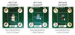
To compare the performance of eGaN FETs and state-of-the-art Si MOSFETs, identical buck converter evaluation boards were designed for the three cases shown in Fig. 12. All of the boards were 4 in.2 (2580 mm2) and had active copper areas of 1 in.2 (645 mm2), outlined in white in the figure. The boards, designed on the same PCB panel to be consistent, had four layers of two-ounce (2.8 mils/70 μm) copper and used the optimal layout discussed earlier.
The 80 V Si MOSFETs used for comparison have CanPAK packages (Infineon BSB044N08NN3), as shown on the left, and the traditional S308 packages (Alpha and Omega Semiconductor AON7280), as shown on the right. For both Si MOSFETs, the lowest commercially available FOM devices for their respective package technologies were selected. A state-of-the-art MOSFET driver (Intersil ISL2111) was used for the MOSFET-based designs. For the eGaN FET based design, an 80 V EPC20214 was used with the Texas Instruments μSMD LM5113 driver. When comparing the eGaN FET and Si MOSFET based designs, the reduced board size occupied by the eGaN FET-based design is obvious, and the eGaN FET design takes up less than half the board space of the MOSFET designs.
12. eGaN FET and Si MOSFET thermal evaluation boards.
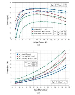
The total system efficiency and power loss comparisons of the eGaN FET and silicon MOSFET based 48 VIN to 12 VOUT buck converters operated at switching frequencies of 300 kHz and 500 kHz are shown in Fig. 13. This plot takes into account losses of the entire system, including the inductor (4.7 μH Coilcraft SER2915L), capacitors, and PCB losses. The eGaN FET based design offers similar light-load efficiency with the S308 packaged Si MOSFET, which has an almost 4× higher on-resistance, demonstrating the low charge of eGaN FETs. At full load, the low on-resistance of the eGaN FET enables much higher efficiency. Combining low conduction losses and low switching losses, the eGaN FET based design has higher efficiency at almost every design point.
The first reason for the improved power density of the eGaN FET based design is that the power device is much smaller in size, when compared to the MOSFET in terms of RDS(ON) times the area.
The second improvement in density is driven by the gate driver, which is also much smaller than its counterpart, in part from better packaging and in part from the reduced drive requirements of low charge, low drive voltage eGaN FETs.
When comparing the eGaN FET and larger CanPAK MOSFET based designs, the performance is improved under all conditions. For the larger, slower switching Si MOSFET the higher switching losses become the major loss mechanism. At a switching frequency of 300 kHz and a load current of 30 A, the eGaN FET based design reduced the total system loss by 35%. At 500 kHz, the eGaN FET based design, with ultra-low switching charges, low on-resistance, and improved packaging, had a minimal drop in efficiency when compared to the MOSFET-based designs. Furthermore, at 30 A, the total system loss was reduced by almost 40% compared to the best Si MOSFET-based solution.
13. Experimental electrical comparison between GaN and Si based buck converters: (a) efficiency and (b) power loss.
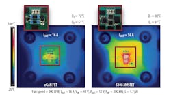
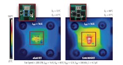
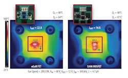
In Fig. 14, the thermal performance of the eGaN FET and Si MOSFET S308 package based designs are compared. At 16 A, the S308 packaged MOSFET design approaches 100°C with an airflow of 200 LFM. The Si MOSFET generates higher power loss from lower electrical efficiency and the package is also less thermally efficient than the eGaN FET chip-scale package, which at the same operating current, has device temperatures 26°C and 36°C lower than the S308 packaged MOSFET, respectively.
14. Experimental thermal comparison between eGaN FET (left) and S308 packaged Si MOSFET (right) based buck converters.
The eGaN FET based design can be operated at the same power levels as the S308 packaged Si MOSFET and run at much lower temperatures. It can also be operated at much higher output powers with similar maximum temperatures. Both of these conditions further improve the power density of the system, which is initially higher from the reduced board space occupied by the eGaN FET based solution.
15. Experimental thermal comparison between eGaN FET (left) and S308 packaged Si MOSFET (right) based buck converters, with same maximum device temperature.
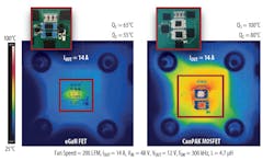
In Fig. 16, the thermal performance of the eGaN FET and CanPAK packaged Si MOSFET-based designs are compared. The eGaN FET is about a third of the size of the CanPAK packaged MOSFET, but still has around half the on-resistance. At 14 A of output current, the CanPAK based MOSFET design reaches 100°C at an airflow of 200 LFM. The MOSFET generates higher power loss from lower electrical efficiency and the package is also less thermally efficient than the eGaN FET, which at the same output current, has device temperatures 35°C and 25°C lower than the CanPAK based MOSFET design, respectively. For the same maximum temperature, the eGaN FET design is operated to 22 A, where the maximum device temperature matches that of the S308 packaged Si MOSFET on the top device (Q1), while the low-side (Q2) eGaN FET runs 13°C cooler, as shown in Fig. 15. The eGaN FET based solution can push almost 40% more output power, while maintaining the same maximum junction temperature. This will enable new levels of performance in traditional power applications.
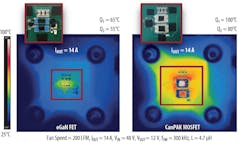
For the same maximum temperature, the eGaN FET based design is run to 22 A, where the maximum device temperature approximately matches that of the CanPAK packaged Si MOSFET, as shown in Fig. 17. The eGaN FET based solution can push almost 60% more output power, while maintaining the same maximum junction temperature, as compared to the Si MOSFET in the CanPAK package.
16. Experimental thermal comparison between eGaN FET (left) and CanPAK packaged Si MOSFET (right) based buck converters.
17. Experimental thermal comparison between eGaN FET (left) and CanPAK packaged Si MOSFET (right) based buck converters.
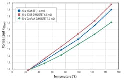
The thermal performance of a device will also impact its electrical performance. The most notable impact on the device as the temperature rises is an increase in the device on-resistance, as shown in Fig. 18. The normalized increase in on-resistance for an eGaN FET and Si MOSFETs are very similar. For a device, the larger the initial on-resistance, the greater the additional conduction losses introduced by higher temperatures.
18. Impact of temperature on normalized device on-resistance.
Due to the lack of an industry standard on test conditions for thermal steady state, it is difficult to compare such data from different sources. As a result, it is common industry practice for efficiency and power loss measurements to use “instantaneous” efficiency measurements. These are not truly instantaneous since the measurements take several seconds, much longer than time constants for typical semiconductor die. However, they reduce many of the heating effects and form a good baseline measurement.
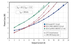
Figure 19 shows a comparison of instantaneous losses measured and thermal steady-state losses with 200 LFM of airflow for a more accurate measurement for real world operating conditions. The eGaN FET based design, which has lower temperatures as a result of lower power loss and the lowest on-resistance, shows a very slight increase in power loss in steady state versus instantaneous cases. The S308 packaged Si MOSFET based design, which has the highest on-resistance, shows a significant degradation in performance in thermal steady state, with power loss increasing almost 20% at 16 A from “instantaneous” to steady state operating conditions.
19. Experimental power loss comparison between eGaN FET and Si based buck converters for instantaneous and thermal steady state operating conditions.
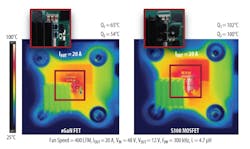
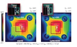
To compare the thermal performance of eGaN FETs and Si MOSFETs with heat sinking, test cases with heat sinks were also evaluated. The heat sinking methods were kept consistent between designs and followed the design process outlined earlier in this chapter. The first comparison was made between eGaN FET and the S308 packaged Si MOSFET based designs, as shown in Fig. 20. The S308 MOSFET, which has very high thermal impedance from junction-to-case, shows little thermal improvement with an increase in achievable output power of 25%. At 20 A, the S308 packaged Si MOSFET approaches 100°C at an airflow of 400 LFM. The Si MOSFET generates higher power loss from lower electrical efficiency and the package is also less thermally efficient than the eGaN FET, which at the same operating current, has device temperatures 37°C and 46°C lower than the S308 packaged Si MOSFET, respectively.
The difference in temperature in this test case is significantly higher than the test case without a heat sink, demonstrating the superior junction-to-case thermal transfer capability of the LGA eGaN FET chip-scale package.
The CanPAK packaged Si MOSFET based design shows less performance degradation in steady state operation than the smaller S308 packaged Si MOSFET, but the CanPAK packaged Si MOSFET still displays a larger steady state operation performance penalty than the much smaller eGaN FET.
20. Experimental thermal comparison between eGaN FET (left) and Si S308 packaged MOSFET (right) based buck converters with heat sinking.
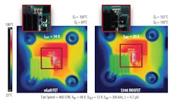
For the same approximate maximum temperature, the eGaN FET based design with a heat sink can deliver 30 A, or 50% more output power than the Si MOSFET based design, before the maximum device temperature approximately matches that of the S308 Si MOSFET operated at 20 A, as shown in Fig. 21. For the eGaN FET based design, an almost 40% increase in output current is achieved with the addition of the heat sink. Looking at the thermal images shown in Fig. 21 it can be seen that the heat sink temperature in the eGaN FET based design is much higher than the S308 packaged Si MOSFET design, indicating much better backside cooling.
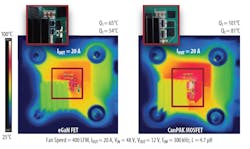
The comparison of the eGaN FET based design and the double-sided cooling capable CanPAK packaged Si MOSFET based design is shown in Fig. 22 for a load current of 20 A. At 20 A, the CanPAK packaged Si MOSFET design reaches 100°C with an airflow of 400 LFM. The eGaN FET based design operating at the same output current, has device temperatures 36°C and 27°C lower than the CanPAK based MOSFET design, respectively.
The CanPAK Si MOSFET occupies around three times the board area of the eGaN FET and shows much better junction-to-case cooling than the S308 MOSFET. The junction-to-case cooling improvement demonstrated by the CanPAK is similar to that of the much smaller eGaN FET, which has a larger thermal impedance introduced by the thermal interface used to attach the heat sink. This is due to the much higher transistor density and smaller surface area to connect the heat sink.
21. Experimental thermal comparison between eGaN FET (left) and Si S308 packaged MOSFET (right) based buck converters with heat sinking, with same approximate maximum device temperature.
22. Experimental thermal comparison between eGaN FET (left) and Si CanPAK packaged MOSFET (right) based buck converters with heat sinking.
For the same maximum temperature, the eGaN FET based design with a heat sink can deliver 30 A, or 50% more output power than the Si MOSFET based design before the maximum device temperature matches that of the CanPAK packaged Si MOSFET operated at 20 A, as shown in Fig. 23.
23. Experimental thermal comparison between eGaN FET (left) and Si CanPAK packaged MOSFET (right) based buck converters with heat sinking, with same approximate maximum device temperature.
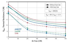
Following the same methodology as earlier in this chapter, the equivalent junction-to-ambient thermal impedances, as shown in Fig. 24, were calculated for the eGaN FET and MOSFET based designs. The eGaN FET based design, occupying the smallest board area, provides the best overall thermal performance. In the case without a heat sink and 400 LFM airflow, the eGaN FET based design has around 9% and 5% lower thermal impedances than the S308 and CanPAK packaged Si MOSFET based designs, respectively. In the case with a heat sink and 400 LFM airfl ow, where the junction-to-case thermal path becomes a major heat path, the eGaN FET based design has around 23% and 5% lower thermal impedances than the S308 and CanPAK packaged Si MOSFET based designs, respectively.
When the superior thermal performance is combined with the improved electrical performance, eGaN FETs can enable unmatched performance, in a fraction of the occupied board space. This is a combination for game changing performance improvements.
24. Comparison of junction-to-ambient system thermal impedance vs. airflow for eGaN FET and SI MOSFET based buck converters.
References
- D. Reusch and J. Strydom, “Understanding the Effect of PCB Layout on Circuit Performance in a High-frequency Gallium Nitride Based Point-of-Load Converter,” Applied Power Electronics Conference and Exposition (APEC), pp. 649-655, 2013.
- D. Reusch, D. Gilham, Y. Su, and F. C. Lee, “Gallium Nitride Based 3D Integrated Non-Isolated Point-of-Load Module,” Applied Power Electronics Conference and Exposition (APEC), pp. 38-45, 2012.
- Efficient Power Conversion Corporation, “EPC demonstration boards.”
- D. Reusch, J. Strydom, and A. Lidow, “Monolithic Integration of GaN Transistors for Higher Efficiency and Power Density in DC-DC Converters,” International Exhibition and Conference for Power Electronics, Intelligent Motion, Renewable Energy and Energy Management (PCIM Europe), pp. 986-993, 2015.
- A. Lidow, J. Strydom, M. de Rooij, D. Reusch, GaN Transistors for Efficient Power Conversion, Second Edition, Chichester, United Kingdom, Wiley, 2014.
- Ralph Locher, “Introduction to Power MOSFETs and their Applications,” Fairchild Semiconductor Application Note 558, 1998.
- “Thermal Design Basics,” Analog devices MT-093 Tutorial, 2009.
- “DirectFET® Technology Thermal Model and Rating Calculator,” International Rectifier Application Note AN-1059, 2010.
