Amplify AC Signals with Large DC Offsets Using an Indirect Current-Mode In-Amp
Members can download this article in PDF format.
What you'll learn:
- Benefits of using an indirect current-mode instrumentation amplifier for large differential offsets.
- Design specs for a low-power application.
- Key design considerations when implementing an in-amp architecture.
- Step-by-step procedure for architecture implementation.
- The process for simulating the in-amp design.
In applications such as electromagnetic-flow (EM flow) meters and biopotential measurements, small differential signals are in series with much larger differential offsets. These offsets typically limit the gain that the circuit can take in the front-end design, which in turn impacts the overall dynamic range. The gain limitation is even more challenging when lower supply voltages are used—for example, in battery-powered signal chains.
One solution to address this large differential offset issue is to use an ac-coupled measurement signal chain. A typical ac-coupled signal chain would include a low-gain instrumentation amplifier, followed by a high-pass filter and additional gain stages. In most applications, it’s preferable to get as much gain as possible at the first stage, as this helps improve the referred-to-input (RTI) noise of the following gain stages in the signal chain.
This article will assist with the design and the implementation of an indirect current-mode instrumentation amplifier (in-amp) architecture, which will enable high gain and ac coupling all in one stage. The design will feature the AD8237, a micropower, zero-drift instrumentation amplifier that has a wide common mode and differential input range. Another example of the indirect current-mode architecture is the AD8420. The main benefits of such an indirect current feedback in-amp are:
- It’s a low-power architecture.
- There’s no diamond plot limitation like with other typical architectures, such as in-amps composed of two or three op amps.
- Good gain drift performance can be achieved from external resistor matching.
- High CMRR can be achieved without relying on resistor matching.
- High-impedance reference pin.
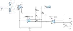
The circuit in Figure 1 provides the overall schematic where the AD8237 indirect current-mode in-amp is chosen. However, to accomplish high gain and ac coupling all in one stage, an integrator circuit has to be implemented in a feedback loop with the AD8237. This solution allows for more gain than instrumentation amplifier solutions composed of two or three op amps, which cancel the offset after gain is applied.
For the proposed architecture, the offset correction happens prior to the gain phase that enables the in-amp to have a large gain. Both architectures will be presented in the appendix. The ADA4505 op amp is used in the feedback loop as the integrator circuit. The output of the AD8237 is sensed by the integrator input and drives the reference pin of the AD8237 to force the output of the AD8237 to VMID, which is set on the +input of the ADA4505.
Even though the integrator circuit provides a low-pass filter function, in this situation, due to its use in the feedback loop, the overall circuit will have a high-pass filter transfer function. Thanks to this behavior, it will ultimately block any dc offsets prior to gain, making it possible to increase the gain further than other solutions. On top of that, it’s even more helpful with low supply voltages and large offsets since the headroom left to work with is limited.
The integrator circuit also forces the output of the AD8237 at a chosen voltage via a reference pin. Indeed, the integrator is forcing the reference pin relative to the FB pin of the AD8237 to be equal and opposite to the differential voltage of the inputs.
Design Specifications Example
For low-power applications, a single supply is usually available, typically somewhere between 1.8 and 3.6 V. The design choices for the circuit shown in Figure 1 depend on the input signal and offset amplitude range and frequency. Table 1 lists example design specifications for this circuit.
The design choices for this circuit were made while using a low-bandwidth mode for the AD8237, allowing for gain flexibility and better stability.
Design Description
The circuit in Figure 1 consists of the AD8237, a micropower, rail-to-rail instrumentation amplifier, and the ADA4505, a zero-input crossover distortion op amp. Both can be powered from a minimum 3.3-V supply (VDD).
This circuit can output a voltage (VOUT), which represents the amplification of the ac signal (VSIGNAL), presented at the input while removing any dc offset voltages (VOFFSET). A VMID voltage is generated to set both the positive input of the ADA4505 and the AD8237 gain-stage output common mode to mid-supply. The VMID is generated with a voltage divider (R1, R2) and buffered by another ADA4505. The AD8237 comes in a mini small-outline package (MSOP) and the ADA4505 is housed in a compact wafer-level chip-scale package (WLCSP).
Design Considerations
1. The positive input of the ADA4505-2 (1/2), VMID, will set the value of VREF (Ref pin of AD8237) and, consequently, the output VOUT. To ensure the maximum output swing between the two supply rails, most instrumentation amplifiers’ optimal value is at mid-supply (+VDD/2) due to the common-mode input voltage vs. output range or diamond plot. A diamond plot tool to help with this will be presented in the design simulations section.
2. When considering the total supply current for the circuit, the choice of resistor values R1 and R2 also matters. The resistor choice is a tradeoff between noise and power dissipation. In the case of this circuit, it’s better to choose larger resistor values to minimize additional supply current. The supply current added for this resistor divider would be:
In the case of the resistor divider (R1, R2), an additional capacitor C1 can be added to bandlimit the noise as well as reduce any 50 Hz/60 Hz or other interference on VDD. The larger the capacitor, the better the noise filtering. However, it will take VMID longer to settle at power-up. The estimated time it takes to settle within 1%:
3. When choosing passive component values (resistors and capacitors), the tolerances should be considered. In the case of the resistor divider (R1, R2), the target VMID value can shift, which would influence the output swing ranges VOUT of the AD8237 and ADA4505.
From the circuit in Figure 1, the transfer function will have two cutoff frequencies that are the result of a high-pass filter coming from the ADA4505 integrator circuit in feedback and a low-pass filter response due to the AD8237 bandwidth. Some gain error can be introduced, which relates to the cutoff frequency of the integrator (ADA4505) in combination with the AD8237 bandwidth. Thus, it’s important that the high-pass cutoff frequency and the low-pass cutoff frequency respect a certain span. Depending on how close cutoff frequencies are to each other, the percentage gain error might change.
4. If the application requires the use of high-impedance sensors, buffers such as the ADA4505 could be used in front of the AD8237 inputs to provide higher input impedance and lower input bias current, as a buffer will convert a high impedance input into a low-impedance output. The AD8237 input bias current is 1 nA maximum over temperature.
Design Procedure
1. Voltage divider for setting VMID:
Using section 2 of Design Considerations for the circuit in Figure 1, the values for the peripheral components are set to R1 = R2 = 1 MΩ to keep the supply-current contribution around 1 µA:
Output of the resistor divider prior to the ADA4505:
Assuming tolerance for R1 and R2 is 5% and taking into account the ADA4505 offset:
To remove ac power-supply interference and noise from resistors, set C1 so the cutoff frequency is at least less than the minimum VSIGNAL frequency of 20 Hz.
Note that the capacitor value can be larger if it’s needed to further bandlimit the noise:
In this case, C1 is set to 22 nF, which provides a frequency of:
2. Instrumentation amplifier (AD8237) gain value VSIGNAL:
Consider that the range span of EM flow sensors’ output typically is a peak-to-peak signal amplitude going from ±75 µV to ±6 mV. For the circuit in Figure 1, the amplitude peak-to-peak signal amplitude range will be set to VSIGNAL = 6 mV peak with a frequency of 30 Hz.
Then, consider the AD8237 output swing range limits to the supply rails. These values can be found in the datasheet from “Output Swing.” Let’s use the case RL = 10 kΩ swing case at +25°C to be conservative:
For a 3.3-V supply:
Since the output is fully differential, the output will swing with respect to VMID will be, worse case:
For positive input signals (VMIDMAX = 1.732 V):
For negative input signals (VMIDMAX = 1.568 V):
Now to set the gain, add up the total expected differential input signals and use the lower of the positive and negative swing ranges to set the max swing range:
Considering the output voltage range limits, the AD8237 gain should be less than 253. To leave some margin for DC errors/others, the gain value for the circuit in Figure 1 should be less than the maximum possible value. There’s also a tradeoff between the gain and the settling time: the higher the gain, the slower the time constant of the filter. Owing to those comments, the AD8237 gain is set to 101.
Note the benefit of design considerations in Step 1 in terms of maximization of the swing value.
From the datasheet, the associated formula for the gain is:
The AD8237 datasheet provides suggested resistor values for gain selection. For the selected gain of 101, the values of these resistors should be RF1 = 1 kΩ and RG1 = 100 kΩ.
3. In-amp (AD8237) bandwidth:
From the datasheet, the cutoff frequency value is:
If the design specification requires a certain minimum attenuation for the maximum signal frequency, this can be easily checked for a given filter cutoff frequency:
4. Setting the high-pass filter cutoff frequency:
A high-value, high-pass filter cutoff frequency set by the integrator can get too close to the cutoff frequency of the low-pass filter set by the AD8237 bandwidth as explained in the Design Considerations section. This will introduce some gain error from the gain established previously.
Assuming ±5% tolerance for R3 and C3, the fastest time constant should be less than the VSIGNAL minimum frequency:
The resistor R3 will have a constant value of 1 MΩ to minimize the current through this resistor into the op amp:
Taking the nearest standard capacitor value to have approximately a cutoff frequency of 20 Hz, let’s set C3 = 1.5 µF, so, the updated cutoff frequency is:
If the design specification requires a certain minimum attenuation for the minimum signal frequency, this can be easily checked for a given filter cutoff frequency. See an example for this circuit:
5. Offset voltage:
Both signals VOFFSET and VCM have limitations.
As expected, the dc offset can be larger than what we usually find in most applications. In this situation, the voltage value must be VOFFSET ≤ ± VMID. If the DC offset is greater than this limit, the VREF voltage value goes outside the voltage supply range of the ADA4505. The equation linked to the reference pin is set to: VREF = VMID – VOFFSET. The VOFFSET will be set at 1 V.
As for the common-mode voltage, it’s directly linked to the VOFFSET value as VCM must be in the range:
If those limitations aren’t verified, the input values of the AD8237 are either over or under the supply ranges. The VCM will be set at 1.65 V.
Design Simulations
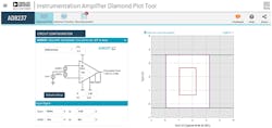
To check the common-mode input range vs. output voltage or diamond plot for an instrumentation amplifier, you’ll want to provide the supply voltage +VDD, reference voltage, gain, common-mode swing, and differential input swing. The instrumentation amplifier diamond plot tool from Analog Devices helps to see if the input swing is within the operating range of the part. Take note that the output swing used for the tool uses the worst-case load conditions (smallest resistive load), so if you design to the tool limits, there would be additional margin for larger resistive loads.
Looking at the results in Figure 2, the purple outline is the usable range of the AD8237 for the given supply voltage, output swing, input common-mode range, and reference voltage of the part. The red outline shows how much of this range you’re using for the given common-mode and differential input mode swing.
The goal is to keep the red outline within the purple outline. If certain conditions violate this, the tool will show the error and provide recommendations. It’s important to note that implementing the integrator circuit in the feedback loop isn’t possible in this interface.
However, a workaround is to configure the diamond plot input signal as if the VOFFSET and VCM voltage of the circuit (in Figure 1) were added in. Hence, using the interval (0.65 to 2.65 V) as the dc offset is removed and isn’t gained up. It also showcases that the common-mode voltage could be higher as there’s still some room for the output to swing. To further understand what’s happening inside the instrumentation amplifier, the Internal Circuitry tab will show the voltages of internal nodes.
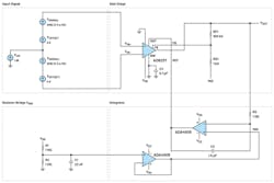
The LTspice simulation tool can check against the design procedure calculations made earlier, including other specifications of interest such as the noise performance in the signal band of interest. The LTspice schematic is shown in Figure 3.
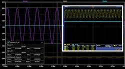
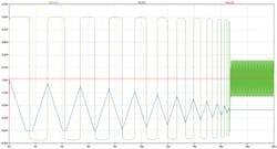
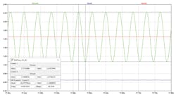
The first simulation (Figs. 4 and 5) is a transient simulation with a dc offset of 1 V and an input signal of ±6 mV at 30 Hz. Figure 4 shows the signal at different stages in the circuit. Figure 5 is a zoomed in version of Figure 4 once the circuit has settled and the integrator capacitor is charged to the final value. The blue curve is the output of the integrator or reference voltage pin of the AD8237. The red curve is the VMID value designed to VDD/2 and the green curve is the final 30-Hz output signal gained, VOUT.
Table 2 shows a comparison of the design goal vs. simulation results for the transient simulation. For the maximum and minimum VOUT value, the expected values come from VOUT = VMID ± VSIGNAL × 101, which in our situation gives us the expected values equal to 2.256 V and 1.044 V. The VREF value expected is equal to VMID – VOFFSET, which gives us an expected value of 0.65 V. As for VMID, we calculated it to be the mid-supply voltage, which in our case is 1.65 V.
The results obtained in the transient analysis compared with the expectations are quite similar in terms of voltage output. However, 17 seconds are needed for the simulation to settle and for the output to get to its final value, due to the large integrator capacitor and the large dc offset implemented. This settling time comes from the fact that the simulation starts at time 0 s, and the capacitor needs time to charge to the final value.
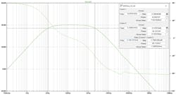
The next simulation in Figure 6 shows the frequency response of the circuit in Figure 3 with a dc offset of 1 V and an input signal of ±6 mV at 30 Hz. Cursors 1 and 2 from Figure 6 were placed at the –3 dB point for the high-pass and low-pass filters, respectively. Table 3 shows a comparison of design goals vs. simulation results.
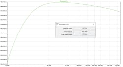
The simulation in Figure 7 shows the voltage noise density vs. frequency RTI for the circuit in Figure 3. This is done by dividing the output noise by the total gain of the solution (101). For the bandpass filter function, we need to choose the integration frequency interval to compute total noise.
For the upper frequency, we will use the sensor maximum frequency value established earlier, which is 220 Hz. For the lower frequency, we will also use the sensor minimal frequency value established at 20 Hz. In this situation, the resulting noise will be from the integration from 20 Hz to 220 Hz.
The measured noise will actually be higher due to the bandpass filter cutoff frequencies. The LTspice simulation results assume a post-processing brick wall filter to have a sharp roll-off at 20 Hz and 220 Hz.
The command line in LTspice is then set to be .noise V(VOUT) V1 dec 100 20 220. Hold the control key and left click on the waveform name (V(ONOISE)/101). The rms noise can easily be converted to peak-to-peak noise using the equation:
A quick check of the AD8237 noise and ADA4505 noise determined that the AD8237 is the dominant noise source.
Measured Results
To highlight the previous results, hardware testing is possible as both the AD8237 and ADA4505 offer test boards. The soldering of each component can be done from the test boards’ schematics. When using both test boards at the same time, a trace on the AD8237 board may need to be cut to connect the VMID voltage to the RG resistors.
To ensure a better understanding, the values of components were set and taken from the design procedure section, the same as with the design simulation. To simulate the EM flow meters or biopotential measurement sensors, different measurement equipment was used, such as a voltage calibrator and an arbitrary waveform generator.
For this test, the input signals were set with a dc offset (VOFFSET) of 1 V, a common-mode voltage of 1.65 V, and an input signal (VSIGNAL) of ±6 mV at 30 Hz.
Looking at the results shown in Figure 8, the output voltage VOUT (yellow curve) performance has a small voltage off from the expected values but is still in line with expectations.
Table 4 shows a summary of design goals vs. measured results.
The differences in the design goal vs. simulation results can have different origins:
- The resistors used had a 5% error tolerance, meaning the VMID value could have been shifted.
- The bench setup may have limitations that can result in minor deviations as shown by the measured simulations, VOFFSET and VSIGNAL.
Tables 5 and 6 present some of the specifications of the devices used in the design.
Conclusion
When capturing signals from sensors such as EM flow in field transmitters or electrodes in biopotential applications, the signal of interest is usually sitting on much larger dc offsets. To make it easier to extract the relevant information from these sensors, one solution is to implement an ac-coupled measurement signal chain. The aim is to remove the dc offsets while amplifying the ac signals.
An instrumentation amplifier like the AD8237 can provide the gain and the ac is coupled all in one stage by incorporating an integrator circuit in the feedback loop. By removing the dc offset at the input stage, this circuit enables maximum signal gain to be applied at the very input of the measurement signal chain. This minimizes the input referred noise of the overall measurement solution.
Appendix
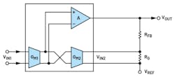
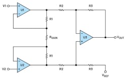
In Figures 9 and 10, the indirect current-mode instrumentation amplifier and the three-op-amp instrumentation are displayed. The indirect current-mode instrumentation amplifier allows for more gain than instrumentation amplifier solutions composed of two or three op amps, which cancel the offset after gain is applied. For the proposed architecture, the offset correction happens prior to the gain phase, which enables the in-amp to have a large gain. Here’s a description of both architectures.
The indirect current-mode instrumentation amplifier in Figure 9 is based on a one-stage configuration. The input voltages are applied to the first GM1 cell, while the GM2 cell is in the feedback loop. The internal integrator Amplifier A forces a replica of VIN1 at VIN2.
The three-op-amp architecture in Figure 10 is based on a two-stage configuration. The first two op amps (U1 and U2), RGAIN resistor, R2 resistors, and R1 resistors form noninverting amplifiers and are considered as the input stage. It provides unity common-mode gain.
The differential gain is set by the resistor RGAIN and equal to:
The last op amp, U3, and the R3 resistors form a differential amplifier that creates the output stage of the instrumentation amplifier. It provides unity differential-mode gain and common-mode rejection. The injection point of the reference for this architecture is at the second stage after the first gain stage is applied.
Acknowledgments
Key consultants for this article were David Plourde, IC Design Engineer, Scientific Instruments (SCI) Group; Aine McCarthy, Lead Systems Applications Engineer, Automotive Group; and Tim Green, Senior Analog Applications Engineer, Scientific Instruments (SCI) Group
References
LTspice: LTspice is a high-performance SPICE III simulator, schematic capture, and waveform viewer with enhancements and models for easing the simulation of switching-regulator, linear, and signal-chain circuits.
Instrumentation Amplifier Diamond Plot Tool: The diamond plot tool is a web application that generates a configuration-specific output voltage range vs. input common-mode voltage graph, also known as the diamond plot, for ADI instrumentation amplifiers.
