This Week in PowerBites: A Surfeit of SiC for Electric Planes, Trains, and Automobiles
This article is part of the This Week in PowerBites Library Series.
What you’ll learn:
- How STMicro is helping Airbus address the challenges of developing hydrogen-electric and hybrid-electric aircraft.
- How a partnership between two wireless power technology leaders is making it easier for developers to find the optimal solution for their application.
- Why a leading GaN manufacturer has suddenly introduced a line of 600-V silicon IGBTs.
Wireless Power Firms Partner to Provide Seamless Short- and Long-Distance Solutions
Two of the world's pioneers in wireless power technology are partnering to create one team that can implement both short- and long-range wireless power designs optimized for each customer's application.
The partnership consists of Powercast, with expertise in long-range over-the-air RF (radio-frequency), and Powermat, which offers its SmartInductive hybrid inductive/resonance short-range power-delivery technology. Both companies will be able to use Powercast's engineering and productization services to support customers as needed from proof of concept to prototyping to production.
Both companies' transmitters (Tx) send energy to receivers (Rx) that convert it into power, but they differ in strength and transfer distance; thus, they fit different applications. Powermat's SmartInductive Tx and Rx must closely align (within eight inches), but they can transfer large amounts of power (5 to 600 W). Powercast's RF Tx and Rx can transfer power over distance (up to 120 feet). However, they deliver lower power levels ranging from hundreds of milliwatts to single-digit microwatts depending on distance.
Powermat's high-power SmartInductive hybrid inductive/resonance technology enables scalable wireless power applications capable of penetrating eight inches of wall and windows. It’s offered in reference-design platforms ranging from 5-W consumer-grade applications to 600-W industrial grade applications like telecom, robotics, micro-mobility, medical devices, and more.
Powercast's RF technology is designed for low-power consumer and industrial devices that need freedom of placement, as they often operate in hard-to-reach places such as IoT sensor networks where wiring and battery replacement would be difficult. RF also enables one-to-many charging, meaning one Tx can charge many enabled devices in its charging zone. Additional device examples include home-automation sensor networks, TV remotes, electric toothbrushes, headphones, and smartwatches.
Rugged 600-V IGBTs Offer High Power Density
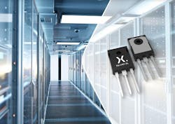
Well-known for its wide-bandgap power devices, Nexperiaadded to that legacy with its unveiling of the NGW30T60M3DF. The 30-A, 600-V IGBT is anticipated to be the first product of a growing family of high-power bipolar devices.
The company says that these IGBTs were developed to address the growing demand for cost-effective, efficient, high-voltage switching devices for power-conversion and motor-drive applications. This includes industrial motor drives like servo motors ranging from 5 to 20 kW (20 kHz), robotics, elevators, in-line manufacturing, power inverters, uninterruptible power supplies (UPS), photovoltaic (PV) strings, EV charging, and induction heating and welding.
The IGBTs feature a robust, cost-effective, carrier-stored trench-gate advanced field-stop (FS) construction, providing exceptionally low conduction and switching loss performance with high levels of ruggedness in operating temperatures up to 175°C.
Designers can choose between the medium- (M3) and high-speed (H3) series IGBTs. They have been designed with very tight parameter distributions, allowing multiple devices to connect safely in parallel. In addition, lower thermal resistance than competing devices enables them to provide higher output power. The devices are also fully rated as soft fast reverse-recovery diodes. As a result, they’re suited for rectifier and bidirectional circuit applications or to protect against overcurrent conditions.
These IGBTs come in a standard, lead-free, TO247-3L package and are HV-H3TRB qualified for outdoor applications. Nexperia plans to follow this release with a series of 1,200-V IGBTs. To learn more, click here.
GaN Driver Integrates Galvanic Isolation for Superior Safety and Reliability
STMicroelectronics’ first galvanically isolated gate driver for gallium-nitride (GaN) transistors, the STGAP2GS, trims dimensions and bill-of-materials costs in applications that demand superior wide-bandgap efficiency with robust safety and electrical protection.
The single-channel driver can be connected to a high-voltage rail up to 1,200 V, or 1,700 V with the STGAP2GSN narrow-body version, and provides gate-driving levels of up to 15 V. Capable of sinking and sourcing up to 3-A gate current to the connected GaN transistor, the driver ensures tightly controlled switching transitions at high operating frequencies.
The STGAP2GS has a very low propagation delay (45 ns) across the isolation barrier that ensures fast dynamic response. In addition, its dV/dt transient immunity of ±100 V/ns over the full temperature range guards against unwanted transistor gate change. The STGAP2GS is available with separate sink and source pins for easy tuning of the gate-driving operation and performance.
Eliminating the need for discrete components to provide optical isolation, the STGAP2GS driver eases the adoption of efficient and robust GaN technology in various consumer and industrial applications. These include power supplies in computer servers, factory-automation equipment, motor drivers, solar- and wind-power systems, home appliances, domestic fans, and wireless chargers.
In addition to integrating galvanic isolation, the driver also features built-in system protection including thermal shutdown and undervoltage lockout (UVLO) optimized for GaN technology, to ensure reliability and ruggedness.
Two demonstration boards, the EVSTGAP2GS and EVSTGAP2GSN, combine the standard STGAP2GS and narrow STGAP2GSN with ST’s SGT120R65AL 75-mΩ, 650-V enhancement-mode GaN transistors to help users evaluate the drivers’ capabilities.
The STGAP2GS in SO-8 widebody package, and the STGAP2GSN SO-8 narrow version, are available now, priced from $1.42 for orders of 1,000 pieces.
Hi-Res Simulation Models Enable Virtual Prototyping with Advanced SiC Power Devices
Navitas Semiconductor and Plexim GmbH have partnered to create a series of high-resolution thermal-loss models. The models enable Plexim's PLECS simulation software to support highly accurate analysis and virtual prototyping of power electronic systems and electrical drives based on Navitas' GeneSiC G3 SiC MOSFET and Gen 5 MPS diode product families.
Power designers can simulate power and thermal losses of Navitas' latest devices in various soft- and hard-switching applications. “Accurate, empirically based simulation models maximize the chance of first-time-accurate designs, accelerating time-to-market and time-to-revenue,” noted Dr. Ranbir Singh, Navitas EVP for the GeneSiC business line.
“The intuitive and highly efficient PLECS lookup-table-based approach to simulating thermal semiconductor losses in complex power electronic circuits is key,” said Kristofer Eberle, Plexim, North America. “Unlike legacy modeling approaches that are not well-suited to new wide-bandgap materials, PLECS uses a simplified but accurate behavioral description to highlight the superior performance of the GeneSiC MOSFETs.”
PLECS models for GeneSiC MOSFETs and MPS diodes are available via genesicsemi.com.
Cool-Running 100-V N-Channel MOSFET Supports Space-Saving Power-Supply Designs
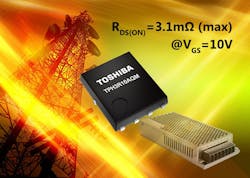
A new 100-V N-channel power MOSFET launched by Toshiba Electronics Europe is based on its latest generation U-MOSX-H process. The new device was created to meet the especially challenging requirements of applications such as switching power supplies for data centers and communication base stations, as well as industrial uses.
Designed for efficient operation, the new TPH3R10AQM achieves a value of just 3.1 mΩ (max.) for the all-important drain-source on-resistance (RDS(on)). This represents a significant 16% improvement over Toshiba’s current 100-V product (TPH3R70APL) that uses the established generation process.
The device offers a drain-source voltage (VDSS) of 100 V and a drain current (ID) capability of up to 120 A. The low gate-switch charge (QSW) enhances efficiency in high-frequency applications, while the elevated maximum channel temperature (Tch) of 175°C reduces the need for thermal management, thereby reducing the size and cost of end equipment.
The new MOSFET expanded its safe operating area (SOA) by 76% when compared with the earlier generation, adapting it for linear mode operation. This enhancement significantly improves its suitability for, and performance in, hot-swap circuitry. Furthermore, as the gate-threshold voltage range is 2.5 to 3.5 V, the device is less susceptible to spurious triggering.
The product uses the highly footprint-compatible SOP Advance(N) package, giving the TPH3R10AQM a PCB footprint of just 4.9 × 6.1 mm.
Shipments of the new TPH3R10AQM MOSFET start immediately.
Ultra-Wide-Input DC-DC Converters Address Railway Infrastructures and Other Demanding Apps
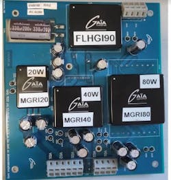
GAIA Converter is expanding its range of high-reliability and industrial-grade wide-input dc-dc converters for rail applications to meet the needs of smart signaling and speed control systems, such as the European Rail Traffic Management System (ERTMS). The upgraded ultra-wide-input portfolio achieves outstanding MTBF (1000 kh at 25°C) performance while satisfying the most demanding surge requirements, allowing for a near seamless modular architecture offering from 5 to 500 W.
The company's latest additions include an input bus conditioner, a device that can suppress extreme surges in railway environments and board-mount parts rated at 20, 40 and 80 W. In addition, the 3-kV ac reinforced safety isolation rating meets the IEC 62368-1 standard.
Outputs available for each model are 2 x 5 V, 2 x 12 V or 2 x 15 V, which are mutually isolated and can be paralleled for higher current, placed in series for higher voltages, or connected as +/- bipolar outputs for maximum flexibility. Efficiency is typically 87% and case operating temperature range is from −40 to +105°C without derating.
The new ultra-wide-input range for each part is 12 to 160 V dc, including 24-, 48-, 72-, 96-, and 110-V dc nominals to meet EN 50155 and other rail specifications, as well as standards for common industrial applications. The input will also withstand 176 V dc for 100 ms to include the surge specified in rail standard NF-F 01-510 for 110 V dc nominal, as well as the RIA12 specification of 168 V dc for 20 ms for 48 V dc nominal.
Surges to 385 V dc for 20 ms to specification RIA12 can be met with the additional input bus conditioner type FLHGI90, which also attenuates fast transients, provides reverse polarity protection, and ensures compliance with EN 550121 EMC specification. Without the input bus conditioner, the parts can meet EN 55022 Class B EMI with a recommended external filter.
Control functions include an on/off pin and output trim, which can vary the outputs from −20% to +10%. Protection features include overload, short-circuit, soft-start, and input undervoltage lock-out, with a trimmable threshold, to match all battery voltage standards. All converters are offered in fully potted, low-profile metallic cases.
For more information, click here.
SiC Schottky Barrier Diodes Meet Higher-Efficiency, Switching-Performance, and Low-Power-Loss Demands
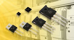
Bourns Inc. announced its first 650- to 1200-V silicon-carbide (SiC) Schottky barrier diodes (SBDs). The SiC SBD line consists of six models engineered to provide excellent current carrying and thermal capabilities and high power density for increased performance and reliability. These capabilities make the devices a good fit for high-frequency applications that must meet reduced size and lower system cost requirements. This includes telecom/server switched-mode power supplies (SMPS), photovoltaic inverters, PC power, and motor drives.
To address ongoing design demands for ever higher power efficiency, the SiC SBDs feature low forward voltage (VF) and high thermal conductivity. This increases efficiency while lowering power dissipation, satisfying application requirements of 650- and 1,200-V solutions. And because there’s no reverse-recovery current, thus reducing EMI, these SiC SBDs significantly lower energy losses.
In addition to offering 650- to 1200-V operation with currents in the 6- to 10-A range, the six new BSD models of wide-bandgap diodes offer designers various forward voltage, current, and package options, including TO220-2, TO247-3, TO252, and DFN8x8.
All six Bourns SiC SBDs are available now. For more detailed product information, click here.
Automotive-Compliant SiC MOSFETs Enhance Automotive Subsystem Efficiency
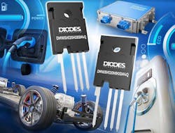
The DMWSH120H90SM4Q and DMWSH120H28SM4Q automotive-compliant silicon-carbide (SiC) MOSFETs are the latest wide-bandgap product offerings from Diodes Inc. These N-channel MOSFETs respond to the growing demand for SiC solutions that enable better efficiency and higher power density in electric and hybrid-electric vehicle (EV/HEV) automotive subsystems like battery chargers, on-board chargers (OBCs), high-efficiency dc-dc converters, motor drivers, and traction inverters.
The DMWSH120H90SM4Q operates safely and reliably up to 1,200 VDS with a gate-source voltage (VGS) of +15/−4 V and has an RDS(on) of 75 mΩ (typical) at 15 VGS. This device is designed for OBCs, automotive motor drivers, dc-dc converters in EVs/HEVs, and battery-charging systems.
The DMWSH120H28SM4Q operates at up to 1,200 VDS, +15/−4 VGS, and has a lower RDS(on) of 20 mΩ (typical) at 15 VGS. This MOSFET is aimed at motor drivers, EV traction inverters, and dc-dc converters in other EV/HEV subsystems. Low RDS(on) enables these MOSFETs to run cooler in applications that require high power density.
Both products have low thermal conductivity (RθJC = 0.6°C/W), enabling drain currents up to 40 A in the DMWSH120H90SM4Q and 100 A in the DMWSH120H28SM4Q. They also have fast intrinsic and robust body diodes with low reverse-recovery charge (QRR) of 108.52 nC in the DMWSH120H90SM4Q and 317.93 nC in the DMWSH120H28SM4Q. Thus, they can perform fast switching with reduced power losses.
Diodes' planar manufacturing process gives the MOSFETs more robust and reliable performance in automotive applications—and with increased drain current, breakdown voltage, junction temperature, and power rings as compared to previously released versions. The devices come in a TO247-4 (Type WH) package, which offers an additional Kelvin sense pin. This can be connected to the source to optimize switching performance, enabling even higher power densities.
The DMWSH120H90SM4Q and DMWSH120H28SM4Q are AEC-Q101 qualified, manufactured in IATF 16949 certified facilities, and support PPAP documentation. The DMWSH120H90SM4Q is priced at $18 in 1,000-piece quantities, and the DMWSH120H28SM4Q costs $38 in 1,000-piece quantities.
SMT Power Inductor Offers High Saturation Current in a Tiny Space
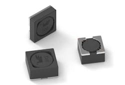
Würth Elektronik's WE-HEPC is the company's smallest nickel-zinc (NiZn)-ferrite-based self-shielded power inductor to date. Thanks to a new and completely automated manufacturing process, these inductors provide consistent high quality and a higher saturation current than any previous of its own or known competitive product, according to the company.
In all, 15 models are available with different attributes (L: 3.3 ~ 100 μH; ISAT: 1.3 ~ 3.3 A) and in package sizes 5030 (4.8 × 4.8 × 1.8 mm) and 6030 (5.9 × 5.9 × 2.85 mm). WE-HEPC is suitable for dc-dc converters, filter applications, embedded computers, and other compact design applications. Due to its AEC-Q-200 Grade 1 rating, it can also be used for some automobile applications. Operating temperature range spans −40 to +125°C. The land pattern is compatible with older WE-SPC and WE-TPC inductors, giving customers a maximum amount of design flexibility.
Like all products in the Electronic Components 2022/2023, the WE-HEPC is immediately available from stock in any quantities. Developers are welcome to request free samples.
Airbus and STMicroelectronics Collaborate on Power Electronics for Aircraft Electrification
Airbus and STMicroelectronics have signed an agreement to cooperate on power electronics Research & Development to support more efficient and lighter power electronics, essential for future hybrid-powered aircraft and full-electric urban air vehicles. An announcement made by STMicro says that the collaboration builds on evaluations already conducted by both companies to explore the benefits of wide-bandgap (WBG) semiconductor materials for aircraft electrification.
WBG semiconductors like silicon carbide (SiC) and gallium nitride (GaN) have superior electrical properties compared with traditional semiconductors like silicon. They enable the development of smaller, lighter, and more efficient high-performance electronic devices and systems, particularly in applications requiring high power, high frequency, or high-temperature operations.
The cooperative venture will focus on developing SiC and GaN devices, packages, and modules adapted for Airbus’ aerospace applications. The companies will assess these components by conducting advanced research and tests on demonstrators, such as e-motor control units, high- and low-voltage power converters, and wireless power transfer systems.
“This collaboration with STMicroelectronics, a global leader in power semiconductors and wide bandgap technologies, will be key to support Airbus’ electrification roadmap,” said Sabine Klauke, Airbus Chief Technical Officer.
Klauke noted that the company's deep expertise in power electronics for automotive and industrial applications would help Airbus accelerate the development of the disruptive technologies required to realize their ZEROe roadmap, a plan to develop the world’s first hydrogen-powered commercial aircraft by 2035. This three-pronged plan includes development of a hydrogen-burning turbofan engine and a high-power electric propulsion system, driven by a hydrogen fuel cell.
STMicro will also support the development of CityAirbus NextGen, an all-electric, four-seat vertical take-off and landing (eVTOL) prototype. Based on a lift and cruise concept, its design will embody many of the lessons learned from two earlier successful eVTOL demonstrators, CityAirbus and Vahana. When complete, the new demonstrator is expected to have an 80-km operational range and a cruise speed of 120 km/h.
In the shorter term, the two companies will explore technologies to reduce the carbon emissions of its existing aircraft, aka "decarbonization." This involves a combination of disruptive solutions that mix new fuel types and disruptive technologies.
One such solution, hybrid-electric propulsion, can improve the energy efficiency of every aircraft class and reduce aircraft CO2 emissions by up to 5%. That figure could be as high as 10% for helicopters, generally lighter than fixed-wing aircraft. Future hybrid- and full-electric aircraft require megawatts of power to operate. This implies huge improvements in power electronics in terms of integration, performance, efficiency, and component size and weight.
To learn more about Airbus's hybridization roadmap, click here.
Read more articles in the This Week in PowerBites Library Series.


