How to Calculate a DC-DC Compensation Network
Members can download this article in PDF format.
What you'll learn:
- The two methods for testing DC-DC stability.
- Frequency behavior with buck VM and CM architectures.
- Compensators for VM and CM architectures.
- Aligning the time constants of the LC filter to close the loop.
When designing a DC-DC converter, components such as FETs, inductors, current-sense resistors, and output capacitors are carefully selected to match desired output-voltage ripple and transient performance. Following the design of the power stage, closing the loop is necessary.
A DC-DC power supply has a negative feedback loop that uses an error amplifier (EA). A signal that travels in a negative feedback system could encounter poles and zeros through its path. A single pole will decrease a signal phase by ~90° and change the gain slope by –20 dB/Dec, while a single zero will add ~90° to the phase and will increase the gain by +20 dB/Dec.
If the phase of a signal is decreased by –180°, a negative feedback loop can turn into a positive feedback loop and oscillate. Keeping the loop stable and avoiding oscillations are design criteria for power supplies.
There are two methods for testing DC-DC stability. The first is frequency response analysis (FRA) in which a Bode plot is created. The second method is a time-domain analysis—a load current transient is performed and the undershoot and overshoot response of the output voltage is observed.
To achieve a stable design, make sure the phase stays away from the –180° phase decrease, called phase margin (PM). This margin should be more than 45°. A 60° phase margin is a good result.
A faster response to current load changes is achieved when the bandwidth (BW) of the power-supply design is wider. The BW of the power supply is where the 0-dB gain crosses the frequency axis (Fig. 1). Also known as the crossover frequency (Fc), the phase at this point is observed to be higher than 45°.
The BW of the DC-DC converter is a derivative of its switching frequency (Fsw) and is usually in the range of Fsw/10 < Fc < Fsw/5. Fsw/5 means a wider BW, which is harder to achieve. The wider the BW, the lower the phase, so there’s a design tradeoff (Fig. 2).
Gain margin (GM) refers to negative gain at Fsw/2 and at –180°, and a –8 dB or higher will provide good attenuation of possible switching noise, or the possibility of gain where phase shifted by –180°. We want to cross the 0 dB point at a –20 dB/Dec slope.
The Power-Stage LC Filter
The power-stage LC filter refers to the inductor and the equivalent output capacitance for a given topology (buck, boost, etc.). Two popular architectures, voltage mode (VM) and current mode (CM), are used for various topologies. The same LC filter behaves differently if used in VM or CM architectures.
Keeping it simple, the LC filter used with a VM adds two poles. In CM, there’s an additional current-sense feedback path that cancels the LC filter double pole. VM is harder to compensate due to the LC double pole that requires more zeros to counter the double-pole effect. Hence, more components are needed.
Buck VM Architecture and LC Frequency Behavior
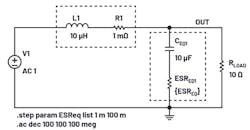
The LC filter adds two poles and a zero caused by the equivalent output capacitance CEQ and its equivalent ESR, ESREQ:
The LC filter double-pole location isn’t related to the LC parasitic resistances. Larger inductance and equivalent capacitance values will cause the double-pole location to be closer to the origin of the frequency axis at 0 Hz. If CEQ and its ESREQ value are higher, the LC filter zero frequency location will move to the left or closer to 0 Hz.
A VM LC filter behavior is shown in Figure 3 and its simulation result in Figure 4. The difference between the red and blue traces is the capacitance ESR value, 1 mΩ vs. 100 mΩ.
Fr has the same location, as LC values haven’t changed. However, the zero location changed due to the change of the ESR value.
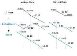
For VM architecture, the LC filter adds two poles and one zero. The frequency response shape is always the same: 0 dB to –40 dB to –20 dB per decade slope. The location of poles and the zero is dependent on the inductance, total capacitance, and the equivalent capacitance ESR values.
CM Architecture and LC Frequency Behavior
The LC filter frequency behavior for CM can be simulated by a voltage-control current source (Fig. 5). The ESR is stepped between two values to show the zero location difference.
The pole location for the LC filter in CM buck architecture is given by:
RLOAD is the load resistance that’s the ratio of output voltage and current. For example, if the output voltage is 5 V and the load current is 2 A, RLOAD will equal 5 V/2 A = 2.5 Ω. The zero location is set by the equivalent output capacitance and its equivalent ESR. Like in the VM architecture, the two values for 1 mΩ and 100 mΩ ESR are:
For CM architecture, the LC filter adds one pole and one zero. The frequency-response shape is always the same: 0 dB to –20 dB to, again, a 0-dB slope (Fig. 6). The frequency location of the pole/zero depends on output capacitance, equivalent ESR, and the load values.
The Compensator
The LC filter causes a phase loss. A compensating network is used to provide a phase boost. It adds poles and zeros to the loop to counter the phase lag, or lead, and gain changes that were caused by the LC filter.
Current-Mode Architecture Compensator
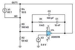
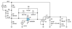
A CM architecture compensator is called a Type 2 compensator (Fig. 7). The AD8038 is the EA, R2 and R3 are the feedback resistors, and R4 is a resistor on which a frequency is injected into the loop by V1 to perform an FRA. The compensation network is formed from R1, C1, and C2.
The expected results for the zero/pole and gain are:
Gain(bzp)—the gain between the zero and the pole—is set by the ratio of R1 to R3. The Gain(rz) is the gain at DC. In these calculations, a frequency of 1 Hz was used for the pole at the origin; therefore, the compensator starts at a –20 dB/Dec slope. Figure 8 shows that the simulation results are in close correlation to the computed values.
VM Architecture Compensator
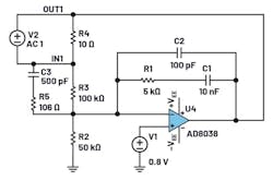
For VM architecture, the compensator has an additional pole/zero combination to counter the additional phase loss of the LC filter. Figure 9 shows a Type 3 compensator network used for VM architecture, and Figure 10 shows its frequency response.
Two additional components, C3 and R5, are placed in parallel with the top feedback resistor, R3. The locations of the pole and the zeros for the Type 3 compensator are:
Note that Fz1(EA) and Fz2 are placed at the same frequency. Sometimes, a Type-3-like compensation scheme is employed. It uses a single capacitor on the top feedback resistor; therefore, the high-frequency pole is excluded, and the compensator slope will continue at 0 dB.
Aligning the Time Constants
One way to close the loop is to align the time constants of the LC filter pole/zero with the compensator’s zero/pole so that they will cancel each other and provide a total of –20 dB/Dec gain slope (Fig. 11).
Using a First-Order Average Model for Aligning Poles/Zeros
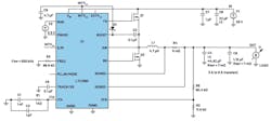
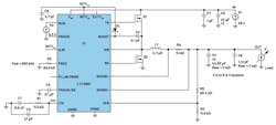
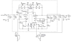
The LTC3891 is a CM controller, which is used for implementing a 28 V to 5 V/6 A. Figure 12 shows the compensation network, on the ITH pin, isn’t aligned with the equivalent output capacitance and its total ESR. This results in oscillations for a transient load test (Fig. 13). The measured switching frequency at the output is 23 kHz and not 500 kHz for which it’s designed.
Combining the two circuits of the power stage and compensator forms a linear circuit that models the closed-loop behavior of a CM architecture.
G1 is a voltage-controlled current source. It has a value of 6, which corresponds to a voltage of 1 V at the plus input of G1 that will provide 6 A at its output (Fig. 14). The frequency response of this circuit has slope changes at different rates and the 0-dB crossover frequency shows 25° of phase (Fig. 15). Therefore, in the time domain, there are oscillations.
To align the time constants, we first need to know CEQ, ESREQ, and RLOAD of the power stage:
R1 is chosen by the designer; here it’s chosen as R1 = 11.5 kΩ, the same as R3 (Fig. 16). R1 × C1(z) = CEQ × RLOAD(p).
Solving for C1:
CEQ × ESREQ (Z) = R1 × C3 (P), the time constant of the compensator’s pole is set by R1 × C3 solving for C3:
A correct simulation result when using this average model shows a –20-dB/Dec slope and phase at 90° (Figs. 17 and 18). If the result differs, it means that the calculations must be verified.
One of the drawbacks of using an op amp as the EA is that it doesn’t correctly predict the BW. Still, it’s very useful to help in verifying the alignment computation. Increasing the BW can be done by increasing R1 resistance value. If R1 is increased, the compensator capacitors need to be decreased by the same ratio to keep the time constants aligned.
There’s a limit to how much R1 can be increased, as a higher gain means a lower phase margin at 0 dB. The phase is always reported as 90° when the time constants are aligned (Fig. 19). The computed values must be verified using the IC switching model and then bench tested for the transient response.
This linear model can be made simpler and more accurate by replacing the op amp with another voltage-controlled current source. The LTC3891 datasheet provides the transconductance value, gm = 2 mmho for 1.2 V. Because G1 positive input is at 1 V, the new value will be 7.2, as 7.2 A/1.2 V = 6 A/V. A simulation of the new circuit (Fig. 20) is shown in Figure 21, and it predicts a BW of 46 kHz.
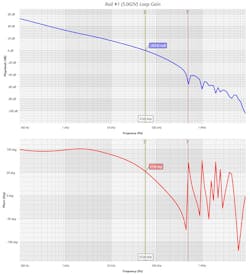
LTpowerCAD predicts a BW of 57 kHz and a phase margin of 52° (Fig. 22). The gain plot looks very similar. The phase starts in a very similar manner but isn’t correctly predicted after 10 kHz.
Right Half Plane Zero (RHPZ)
RHPZ is zero that adds 20 dB of gain and reduces the phase by ~90°, making it impossible to compensate. It’s a limiting BW factor for topologies like boost, buck-boost, and SEPIC that work in continuous-conduction mode. The frequency location of the RHPZ is calculated by:
Usually, the inductor selection is the only variable in these equations where a designer can make tradeoffs. The RHPZ location limits the BW of the design as the loop needs to be closed at a frequency that’s F(RHPZ)/10. The linear model circuits offered here don’t take that RHPZ into account.
Voltage-Mode Buck-Boost Example
The LTC3533 is a VM architecture buck-boost regulator (Fig. 23). When in boost mode, the limiting factor will be its RHPZ. The LTC3533 demo board is configured 3.3 V/1.5 A when input is at VIN(MIN) of 2.4 V. In this case, the duty cycle (D) will be D = (Vo – VIN)/Vo = (3.3 – 2.4)/3.3 ≈ 0.27. RLOAD = VOUT/IOUT = 3.3/1.5 = 2.2 Ω.
The RHPZ location can be found by either of its equations:
A safe place to close the loop will be at 8.4 kHz. Rt sets the switching frequency Fsw = 1 MHz. Note that this compensation is a Type-3-like compensation, as RFF is missing. Thus, Cff doesn’t contribute the additional high-frequency pole.
The locations for the poles and zeros are:
The double-pole location of the LC filter is at 15.65 kHz. The two zeros, Fz1 and FzCff, are placed together at ~9 kHz to counter the poles of the LC filter. Also, the zero that’s formed from the LC filter at 967 kHz has a pole to counter its effect at 896 kHz.
An average LTspice circuit for VM architecture that uses an op amp as the EA can be used to check the alignment of poles and zeros (Fig. 24). A simpler circuit can be used by utilizing a voltage-control voltage source as the EA (Fig. 25). Its gain value is derived from the Error Amp AVOL specified in the datasheet, which is 80 dB. 80 dB = 20log10000. Thus, for the simulation, a value of 10000 is used.
The simulation of both circuits provides a very similar solution (Fig. 26). The BW hasn’t changed like that seen in the CM circuit simulation. The gain is very similar and the phase is forecasted at 90°, but this only provides information on the correct alignment. There’s an additional capacitor of 188 μF as well as a 0.2-Ω resistor at the output.
As seen in Figure 4, a voltage-mode LC filter can generate a high Q, especially when ESR and DCR are low in value. To make sure that the LC filter is properly damped, an additional RC is added to the output. It’s computed by:
Conclusion
LTspice circuit simulation offers an efficient and reliable way to verify calculations for compensation networks.1 While the linear model discussed doesn’t include the current-sensing element, its signals’ gain, or RHPZ information, the benefits include fast simulation speed and compatibility with various DC-DC topologies. In addition, the output displays a –20-dB/Dec gain slope along with approximately 90° of phase if correct results are achieved.
References
1. Henry J. Zhang. “Modeling and Loop Compensation Design of Switching Mode Power Supplies.” Analog Devices Inc., January 2015.
“LTspice Simulation Files for Power Stages and Average Compensation Models.” Analog Devices Inc.
