Exploring Uncommon Applications of Isolation
Members can download this article in PDF format.
What you'll learn:
- Signal and power isolation using a DC-DC converter implementation.
- The importance of isolation in medical equipment.
- A self-driven synchronous-rectifier circuit to isolate high voltage.
One of the main reasons that a circuit may need isolation is to protect it from damaging or dangerous currents and/or voltages. Isolation will also prevent dangerous voltages from passing to the operator during an electrical fault/failure or lightning surge. However, the flow of AC current transfer of power and signal will still be able to flow between two circuit system areas.
This article describes some various application examples that need isolation. Here are only a few general examples:
- Protecting human operators and low-voltage circuitry from high voltages.
- Improving noise immunity.
- Handling ground potential differences between communicating subsystems.
Now let’s get down to some of the key areas that use isolation.
Integrated Signal and Power Isolation1
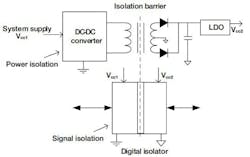
Isolators with complementary metal-oxide semiconductor (CMOS), or transistor-transistor logic (TTL) level inputs and outputs, can be defined as digital isolators. Digital isolators provide signal isolation. However, complete isolation of the two voltage domains will require power isolation as well.
Figure 1 demonstrates a traditional method that will generate isolated power using a DC-DC converter that will drive a transformer with either flyback, push-pull, or fly-buck topologies.
Benefits of integrated signal and power isolation include:
- Reduction of circuit board area.
- Ease of certification: Having more discrete isolation components will add to the customer’s time required for safety-related certification at the system level. An integrated solution has both signal and power isolation, which is able to be certified together according to component standards like Verband der Elektrotechnik (VDE) 0884-11 and Underwriters Laboratories (UL) 1577. This method will lead to a shorter certification process for the end product.
Medical Isolation
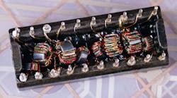
One of the key areas of minimizing electromagnetic interference (EMI) is the electrical isolation of medical equipment via the use of high-quality electrical components. These will allow for safe galvanic separation between primary and electrical circuitry.
Medical isolation will limit the risk of electrical leakage as well as minimize any interference to other nearby devices. Such isolation will also safeguard the device it may be integrated into from any power-quality problems that may be affecting the network.
Isolating transformers can be easily integrated into just about any medical equipment design architecture, such as magnetic resonance imaging (MRI) and surgical robots. Design engineers will now be able to play a key role in helping their device designs to meet the stringent European Union (EU) requirements for medical technologies.
We can think of isolation as a device being quarantined from any network. The intent is device safety and the safety of users, just like a patient being connected to medical electronic equipment. Good isolation will make the rest of the electrical network remain healthy and stable.
Self-Driven High-Voltage Isolation Circuit2,4
Designers can employ a blocking FET to isolate high voltage. However, an external capacitor will be needed to lessen the impact of a high dv/dt. This will introduce an additional sampling delay. A self-driven synchronous rectifier (SR), drain-to-source voltage-sensing circuit, is verified and proposed. This circuitry can provide a low impedance bypassing path for the current that’s introduced via a high dv/dt. In addition, digital isolators and filters will also introduce additional delays.
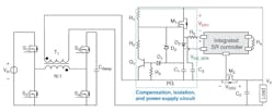
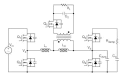
Figure 2 proposes an SR IC that’s implemented in a bipolar process, enabling a low delay and a high driving current density. This new type of peripheral circuit can just about eliminate the dead time, isolate the high voltage, and power up the SR IC—all at the same time.
When employing a 200-W, double-clamp zero-voltage-switching (DCZVS) buck-boost converter prototype, the proposed SR in Figure 2 enables a switching frequency of greater than 700 kHz while achieving a minimal dead time. In this case, the turn-on propagation delay, which includes peripheral circuitry, and SR IC will be reduced to 8.1 ns. The isolated drain-source voltage will be limited to only 10 V, and the peak efficiency is 93.6%.
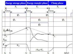
The DCZVS converter design in Figure 3 is set up in three phases:
- The energy storage phase (T1)
- The energy transfer phase (T2)
- The clamp phase (T3)
The efficiency of the flyback converter can be improved with a secondary-side resonance scheme that’s proposed to shape the primary current waveform. This scheme significantly reduces the primary root mean square (rms) current. To further enhance the efficiency of energy transmission, a damping resonance scheme is used.
Optimization Method of the DCZVS Converter
To analyze the ZVS transient process during the ZVS phases (TZVS1 and TZVS3), there’s one proposed method that will achieve sufficient freewheeling current without current sampling.
Secondary-resonance and damping resonance can now be analyzed so that designers will be able to reduce the conduction loss during the energy transfer phase with optimally designed passive devices.
Without making the control more difficult (Fig. 4), ZVS efficiency and effectiveness are improved by increasing control of the two passive devices (CZVS and Rdamp).
The experimental results of the DCZVS prototype were constructed to have the highest frequency of 1 MHz. To reduce the conduction loss of the secondary side, the four MOSFETs (Q1 through Q4) are connected in parallel as shown in Figure 4.
Challenges in High-Voltage Design with Isolation6
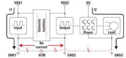
Galvanic isolation serves to partition electrical circuitry by preventing the DC power flow, along with unwanted AC power, while enabling the signal and power transfer across the isolated partition.
In Figure 5, we find that Ground 1 (GND1) is galvanically isolated from Ground 2 (GND2). This means that there’s no common DC GND current that passes through the isolation barrier.
References
1. “Fully integrated signal and power isolation – applications and benefits,” Vikas Kumar Thawani, Anand Reghunathan, Texas Instruments, 2017.
2. “A High-Speed Synchronous Rectifier With Improved Dead Time Compensation and Suitable for High-Voltage Applications,” Minggang Chen, Yongjia Li, Senior Member IEEE, Jiawei Shi, Song Ding, Zhongyuan Fang, Shen Xu, Member IEEE, Qinsong Qian, Member IEEE, and Weifeng Sun, Senior Member IEEE.
3. “Design and analysis of high-voltage blocking in drain–source synchronous rectifier controllers for kV operation,” O. Yu, C.-W. Chen, C.-S. Yeh, and J.-S. Lai, IEEE J. Emerg. Sel. Topics Power Electron., vol. 8, no. 4, pp. 4406–4415, Dec. 2020.
4. “A Novel Realization of ZVS and Efficiency Optimization for Double-Clamped ZVS Buck-Boost Converter without Current Sampling,” Song Ding, Tingying Wang, Qi Liu, Yuanhang Zhou, Qinsong Qian, IEEE 2022.
5. “A ZVS Branch-Sharing Partial Power Converter With Bipolar Voltage Regulation Capability,” Wenjing Xiong, Member, IEEE, Mingdong Wang, Guangfu Ning, Member, IEEE, Yao Sun, Member, IEEE, and Mei Su, Member, IEEE, IEEE Transactions on Industrial Electronics, Vol. 71, No. 2, Feb. 2024.
6. “Addressing high-voltage design challenges with reliable and affordable isolation technologies,” Krunal Maniar, Steven Mappus, Tim Merkin, Alex Triano, Luke Trowbridge, Texas Instruments, 2023.
7. Data Isolation, COHESITY.
