GaN Power ICs Push Power Density with Double-Sided Cooling
Check out Electronic Design's coverage of APEC 2024.
Texas Instruments (TI) aims to push the limits of power density with new 100-V gallium-nitride (GaN) power stages.
GaN is all the rage in the world of power electronics after decades of domination by silicon. The material has gained ground in recent years due to its many superior characteristics, namely reductions in gate charge (Qg), output capacitance (COSS), and reverse-recovery loss (QRR). These qualities all curb power losses when it’s necessary to distribute or convert power from one form or level to another.
Higher switching frequencies with GaN give you the ability to use smaller inductors, capacitors, and other passives, as well as transformers and magnetics, saving space and costs on the final printed circuit board (PCB).
TI takes advantage of these power-handling properties in its new 100-V series of GaN power stages with dual-side cooling: the LMG2100 and LMG3100. The fast switching speeds and low power losses of GaN give them the ability to reduce the area of mid-voltage power supplies strapped to solar inverters and data centers by north of 40%, said David Snook, TI’s head of product management for GaN power.
He added that swapping out silicon MOSFETs for the new GaN power FETs cut switching power losses by 50%. TI also integrated the GaN FET in the same dual-side cooling package as the gate driver, contributing to a power density of 1.5 kW per in3.
Integrating the switch and gate driver further reduces switching losses, as the smaller power loop and gate loop inside the package help reduce parasitics, said TI. The power stages contain a single GaN FET or dual GaN FETs in a half-bridge configuration along with the gate-driver IC.
According to the company, the GaN power FETs can fit inside virtually any mid-voltage power supply. But the biggest impact may apply to power supplies used to feed power to high-end processors and AI chips in the data center.
TI put the chips on display for the first time at this year’s Applied Power Electronics Conference (APEC).
The Power Delivery Dilemma of AI Servers
The latest AI accelerators, such as NVIDIA’s H100 GPUs, consume up to 700 W of power. But since they use relatively tiny supply voltages, each requires hundreds to thousands of amps of current, said Snook. This drives up power-per-rack specifications to 90 kW, up from 15 to 30 kW per rack at present. As power demands in data centers grow by up to 3X, delivering more power in a smaller space is vital.
When power enters the data center from the grid, one of the core building blocks it encounters before entering the processor is a switch-mode power supply (SMPS). The SMPS converts the high-voltage power distributed to columns of servers—120 or 280 V AC—to a lesser DC voltage that can be safely used by the PCB where the processor is housed. For a long time, 12 V was the standard DC voltage output by one of these power-supply units (PSUs), but technology giants have been upping their standards to 48 V.
The key to minimizing power loss is to deliver power at higher voltages and lesser currents and then step down the voltage as close as possible to server silicon. Since Ohm’s Law states power is equal to current times voltage (P = I × V), upping power delivery to 48 V from 12 V means 4X less current is used, reducing excess power losses due to resistance on the power rails. According to the other form of Ohm’s Law, which states power equals resistance times current squared (P = R*I2), power losses drop by 16X.
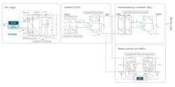
With the power demands of data centers on the rise, TI said standard silicon MOSFETs are no longer cut out for converting and regulating the power to the servers due to excess power losses. TI said GaN power ICs the likes of the LMG2100 and LMG3100 can reduce these losses—and and, therefore, the cost and carbon footprint of data centers—in the synchronous rectifier on the secondary of the LLC stage. The LMG2100 and LMG3100 also have very low on-resistances (RDS(on)) of 4.4 mΩ and 1.7 mΩ, respectively.
TI said the GaN FETs are ideal for intermediate bus converters (IBCs), which are growing more widespread as the power delivery network (PDN) in data centers upgrades to the 48-V bus. The IBC is used to convert the intermediate 48-V voltage from the output of the power supply to a lesser voltage, which then flows into the server itself. It helps reduce I2R losses when distributing power to the server, which gives you the ability to reduce the size and cost of busbars and power-carrying wires in servers, according to TI.
The drawback of the IBC is that it adds another step to power conversion that can dent efficiency. High-efficiency GaN power stages such as LMG2100 and LMG3100 can minimize the tradeoff, said TI.
The power supply and the bus converters are the final step before the power enters a voltage regulator, which in various ways steps down the 12- or 48-V DC input voltages even further to run the processor or accelerator in the server.
Packaging Brings Dual-Side Cooling to GaN
TI said, in the context of a 48- to 12-V DC-DC converter, the 100-V GaN power ICs can drive the system efficiency to 98% or higher. This is primarily due to their 60% reduction in output capacitance and 50% in gate-drive losses.
One of the other unique features of TI’s GaN power FETs is its thermally enhanced dual-side cooled package. The standard cooling on the top of the package coupled with its extended bottom-side ground pad enables more efficient heat removal from both sides of the PCB at the same time, improving thermal resistance, said TI. This makes a major difference for solar inverters and other passively cooled systems.
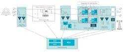
The GaN power stage ICs are also appropriate in other areas, including solar inverters, according to the company. In this case, higher power density and efficiency enable the same solar panel to store and produce more power in a much smaller footprint.
A pair of subsystems form the power-delivery backbone of every solar panel. A boost PFC stage followed by an inverter converts a DC voltage range to AC voltages used by the electric grid. Then, in a buck-boost stage, a DC-DC power converter translates a varying DC voltage to a common DC voltage using maximum power-point tracking (MPPT) that can then be delivered to a string inverter.
"For power-supply designers, delivering more power in limited spaces will always be a critical design challenge," said Kannan Soundarapandian, GM of High Voltage Power at TI.


