For a recent design project, a robust power supply was needed to control the gates of high-side FETs. Optocouplers readily translate the logic signals up to the correct control voltages to drive the FETs. However, to ensure that the FETs turn on and off cleanly, the design required a solid –15 V relative to a wildly floating high-side rail.
A simple Zener diode and resistor, possibly with a FET buffer to ensure adequate current, might do the job under some conditions. In certain circumstances, though, the required gate drive would dip slightly below the lowest other supply rail in the system, which is in this case Gnd, since there are no negative supplies. At other times, it could be almost 100 V above all other supply voltages. Since the design in question was to be used in a production scheme, the solution had to stay away from proprietary, expensive, single-source parts.
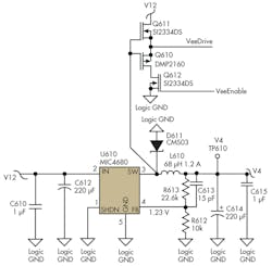
The design already included a switching supply to efficiently convert from an incoming supply at approximately 12 V, down to an internal logic supply at 4 V (Fig. 1). The switch node of that supply, at the junction of U610 pin 3, L610, and D611, swings between the incoming 12-V rail and a diode drop below ground—approximately –0.5 V. This could provide the feed for a charge pump. However, the 4-V supply can’t be lightly loaded, which would cause insufficient drive at this point to support a charge pump.
1. The 12-V downswitcher, which is already in the design, provides a square-wave to generate VeeDrive from V12 with about a 10-V swing.
To guarantee a solid drive for the charge pump, power is derived directly from the 12-V supply and ground using transistors Q610 and Q611. Note that these aren’t configured in a traditional inverter configuration, which could suffer from shoot-through when both are turned on simultaneously during the gate’s voltage transition.
Instead, transistors Q610 and Q611 are simple source-followers. As the gate voltage rises more than about a volt above the present value of net VeeDrive shown in Figure 1 at the source terminals of Q610 and Q611, Q611 turns on, pulling up VeeDrive so it remains about 1 V below the gate voltage all the way up. On the falling edge at the switch node, the gate voltage falls, Q611 is turned solidly off, and Q610 begins to turn on as the gate voltage falls about 1 V below VeeDrive. Therefore, VeeDrive follows the gate voltage down to within about 1 V of Logic GND.
As a result, VeeDrive provides a sharp and muscular square-wave that swings between about 1 V and 11 V (relative to Logic GND), for a total of 10 V p-p. It’s robust enough to drive several charge pumps, if the need arises for multiple supplies. In fact, this one square-wave provided all four supplies required by the design at hand.
Q612 is an optional component. Raising net VeeEnable, the gate drive to Q612, to a logic high voltage turns on Q612 and enables the charge pump action. Lowering VeeEnable back to Logic GND turns off Q612 and disables the low-side drive, allowing VeeDrive to settle to a steady state just below V12. This will save power during those times that don’t require the GateDrive supply.
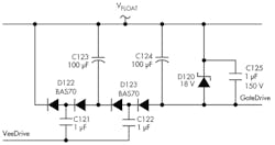
Figure 2 shows one of the four charge pumps using VeeDrive to provide a floating supply that follows a specific floating rail VFLOAT. Because the gate drive must be at least 10 V below VFLOAT, and some drops occur in the diodes, a two-stage charge pump is employed. My actual design includes four copies of the charge pump shown in Figure 2 to produce GateDrive relative to each of four different floating supply rails. A single VeeDrive drives all four rails.
2. The charge pump generates a robust supply that always tracks 15 V below VFLOAT, even if that voltage is below ground. The voltage also can be placed above VFLOAT by simply reversing the diodes and the polarized capacitors
Starting with accumulators C123 and C124 discharged, when VeeDrive goes low (1 V), C121 charges up through C123 and the right half of dual diode D122 to approximately VFLOAT – 1.5 V (after accounting for an approximate 0.5-V drop of the diode). When VeeDrive goes high (11 V), C121 discharges through the left half of D122 to VFLOAT – 10.5 V (11 V – the 0.5-V drop in the diode). As cycling continues, charge continues to be drawn through C123, gradually charging up C123. In steady state, with no current being drawn off, C123 will charge up to 9 V, leaving its negative end at VFLOAT – 9 V.
The second-stage charge pump, consisting of C122, D123, and C124, operates similarly to produce an additional 9-V offset. As a result, GateDrive is 18 V below VFLOAT. In actual practice, of course, some current is being drawn off and there are more resistive drops, so the actual voltage settles close to 15 V. Should the voltage somehow exceed 18 V, Zener D120 clamps the voltage to no more than 18 V, which guarantees that the GateDrive’s 20-V maximum limitation isn’t surpassed. C125 helps to suppress switching noise caused by sudden loads on the supply during switching.
This arrangement can be readily adapted to many situations. If VFLOAT can change, even fairly rapidly, the large size of accumulators C123 and C124 relative to flying capacitors C121 and C122 ensures that GateDrive maintains a fairly constant offset from VFLOAT. This will hold true while the flying capacitors rapidly charge or discharge to the appropriate levels to continue the charge pump action.
Because the flying capacitors are ceramic (and thus unconcerned about polarity), GateDrive will remain 15 V below VFLOAT, even if VFLOATshould fall all the way to Logic GND or below. The flying capacitors must, however, have a sufficient voltage rating so that the highest value of VFLOAT can occur in practice.
The output voltage at GateDrive is very consistent in practice and nicely matches the theoretical values after accounting for the various drops in the feed. There are several ways to adjust this voltage, though. Stages can be easily added to or removed from the charge pump to produce different multiples of the input voltage. If the input voltage is adjustable, finer granularity is possible.
It’s easy to configure GateDrive when it must be above rather than below VFLOAT. Simply flip the polarized accumulator capacitors to allow for the new state, and reverse the diodes. With those simple changes, the design will produce GateDrive at approximately VFLOAT + 15 V.


