>> Electronic Design Resources
.. >> Library: Article Series
.. .. >> Series: Ideas for Design
.. .. .. >> Ideas for Design Vol. 1
Download this article as a PDF file
Systems incorporating microprocessors, FPGAs, ASICs, and other expensive devices can sustain costly damage if the power supply voltages exceed the nominal values. Rather than hoping for the best, good design practice says you should add circuitry that will indicate an overvoltage (OV) condition, take corrective action, take protective action, or perform a combination of all of these functions.
The OV indicator can be an audible or visual alarm. Correction can take the form of additional active circuitry that adjusts or clamps the higher-than-normal voltage. Protection usually involves forcibly shutting down the power supply.
To decide if an OV condition exists, you will probably want to use a separate, standalone detection circuit with an accurate trip-point. The advantage of a standalone detector compared to a power supply that detects its own overvoltage condition becomes clear if a failure mode effects analysis is performed. With separate circuitry, a single-point failure can be prevented from causing an overvoltage condition.
To get an accurate trip-point, avoid using Zener diodes. They generally have poor initial accuracy, an undesirable temperature coefficient, and an undesirable voltage versus current characteristic (a soft knee). A voltage reference diode/IC or a voltage monitoring IC will provide better results. These devices usually feature an accurate, stable comparator and an accurate voltage reference, and they may include on-chip voltage divider resistors. Designers can also add voltage divider resistors external to the IC. If so, they should be accurate (1% tolerance or better) resistors with a low temperature coefficient.
The Intersil ISL6132 is an easy to use, flexible voltage monitoring/supervising IC. It has two comparators intended for undervoltage detection, two comparators for overvoltage detection, and an accurate reference voltage. This application uses the two OV detectors to implement two of the three previously described functions: indication and protection.
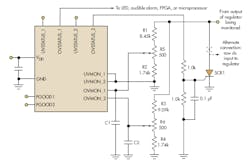
The divider resistors are R1 and R2 (upper and lower resistors, respectively), which set the overvoltage trip-point for the ISL6132’s OVMON_1 input, and R3 and R4, which set the overvoltage trip-point for OVMON_2 (Fig. 1). For example, assume the system operates with a 3.30-V dc bus. Then assume we want an alarm indication to occur if the supply bus voltage rises to 3.40 V dc, and we want to take protective action if the voltage rises to 3.60 V dc.
1. The overvoltage protection circuit employs two voltage divider circuits that set the overvoltage trip points for the voltage monitoring/supervising IC, inputs OVMON_1 and OVMON_2.
The voltage dividers reduce the applied voltage to match the ISL6132’s internal reference voltage. The internal comparators act when the applied voltage just exceeds the reference voltage. Assuming that the input current to the comparator is negligible, and the reference voltage is typically 633 mV, the standard voltage divider formula provides the resistor values:
VOut = VIn – R2/(R1 + R2)
where VOut is 633 mV, and VIn is 3.40 V or 3.60 V. If you select R2 as some standard value, e.g., 2.00 kΩ, you can calculate R1.
For the 3.40-V detection circuitry, R1 is 8.74 kΩ. For the 3.60-V detector, R1 is 9.38 kΩ. For practical purposes, pick the nearest 1% values. To add some adjustment range in the trip-points, insert a trimmer potentiometer between the upper and lower resistors (Fig. 2).
2. The addition of trimmer potentiometers to the divider circuits provides the ability to make makes adjustments to the trip points. The divider resistors’ values should be modified to account for the potentiometers’ values.
For example, use a 500-Ω trim-pot and subtract 250 Ω from each of the upper and lower resistor values. Then, pick the nearest standard value. The result is 8.45 kΩ, 500 Ω, and 1.74 kΩ for the 3.40-V divider and 9.09 kΩ, 500 Ω, and 1.74 kΩ for the 3.60-V divider.
Those who would prefer to avoid algebraic manipulation can use an alternative method for calculating the divider resistor values. As before, assume you want to get a specific output voltage, VOut, from the divider with a specific input voltage, VIn, and that the input current to the comparator is negligible (Fig. 3).
3. An alternative method of determining the voltage divider resistors involves using the known voltages, VIn and VOut, and simple Ohm’s law calculations.
Select the lower resistor, R1, as some convenient value—1.0 kΩ, 10 kΩ, or such. Using Ohm’s law, calculate the current through that resistor: VIn/R1. This is also the current through the upper resistor, R2. The voltage across R2 is VIn less VOut. R2 can then be calculated using Ohm’s law.
If you want to minimize the response to very narrow voltage transients, you can add small capacitors (C1 and C2) between the potentiometers’ wipers and the circuit’s common ground (Fig. 4). Typically, 1 nF to 0.1 µF is sufficient. Since the circuit does not use the ISL6132’s undervoltage detection inputs (UVMON_1 and UVMON_2), they should be connected to the circuit’s common ground.
The device’s overvoltage 1 output (OVSTATUS_1) can be used to light an LED, energize an audible alarm, or provide an input to an FPGA or microprocessor. The overvoltage 2 output (OVSTATUS_2) can be used to shut off the monitored power supply. The preferred implementation (usually called a crowbar circuit) consists of a silicon controlled rectifier (SCR) connected across the power supply bus being protected. OVSTATUS_2 triggers the SCR’s gate. The gate should be bypassed with a 0.1-µF capacitor so the SCR isn’t triggered by the rapid dv/dt of the supply bus at power-up.


