Many electronics circuits begin operation at voltages below 1.25 V. But popular adjustable regulators such as the LM317, LM350, and LM338 can provide output voltages only above 1.25 V, and the L200 minimum is higher at 2.85 V. Fixed-output regulators in the 78XX and LM29xx series start at 5, 3.3, 3.0, 2.85, or 2.5 V.
The approaches shown here allow you to provide near-zero and 0-V output (sometimes called “ground-level”) from these regulators. There are two ways to achieve this: subtracting a reference voltage from the output of the regulator, or offsetting the voltage adjustment resistors of the regulator.
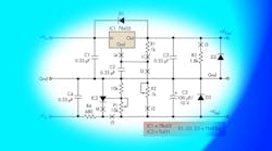
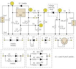
Figure 1 implements the first approach, where the reference source with voltage to be subtracted via a “voltage-reducing block” is connected between points 3 and 4 of the circuit. The choice is made according the required output current, voltage, and temperature stability. There is no need to subtract exactly 1.25 V or a similar voltage.
Among the components that can be used between points 3 and 4 are: one or more diodes (e.g., 1N400X or 1N540X); one or more Schottky diodes (1N5819, 1N5822); reference diodes (LT1004-1.2, LM385-1.2, TLVH431, TLVH432, LM336-2.5, ADR512, LM4041c12); reference shunt regulators (TL431, LM431); Zener diodes (1.3 W series); LEDs (all colors or combinations, as their voltage drop and current ratings differ); and even transistors used as Zener diodes or as simple diodes.
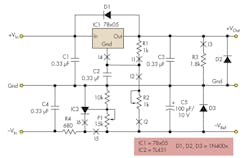
Each of these solutions has advantages and drawbacks. For example, with the TL431 you can achieve 100-mA output current and good temperature stability. (In that case, voltage V3 at point 3 should start at 2.5 V.) R1 and R2 are standard voltage adjustment resistors for regulators such as the LM317 and LM350.
R3, R4, and R5 are optional. R3 is a current-limiting resistor, which can be eliminated if not needed and replaced by a jumper J1. R4 can provide the minimal load current for the regulator IC1. Most often, R1 and R2 provide that current, but that is not required and is not always a good option. R5 can provide the minimal load current for the regulator IC1 and/or the minimal current for the subtracting element connected between points 3 and 4.
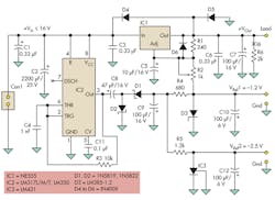
The second approach is useful where circuits operate from a single power supply, such as 6-V or 12-V rechargeable batteries, and the input power supply is usually limited to around 16 V (Fig. 2). In these cases, you reduce and offset the output voltage of the LM317x by offsetting the voltage-adjustment resistors.
An NE555 and associated components can be used to produce a negative voltage. Here, it produces –1.2 V for the offset of LM317x and –2.5 V for the analog circuits in the system. The working frequency of the oscillator is usually set between 20 kHz and 200 kHz. D1 and D2 should be fast-switching diodes with low-voltage drop such as the 1N5819 or 1N5822. D3 is a voltage-reference or parallel voltage regulator providing the offset, such as the LM385-1.2 V. Resistor R6 is optional. It provides most of the minimal load current for IC1, if needed.
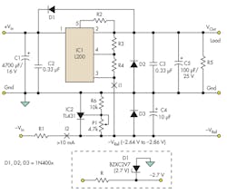
In Figure 3, a shunt regulator such as a TL431 drives the output of the adjustable L200 regulator to ground. It should be rated at 10 mA or more to sink the current from the L200. Trimming potentiometer P1 provides appropriate bias voltage for the L200. Also, –VRef should equal the internal voltage of the L200, which is specified to be between 2.64 V and 2.86 V. Resistors R2, R3, and R4 are calculated according to the datasheet and the application note for the L200.
This method also can be applied to adjustable regulators of the 78xx series (Fig. 4). Trimmer P1 is used to make the reference voltage –VRef equal to the output voltage of 78X05 and thus yield output voltage +VOut close to ground. R2 adjusts output voltage +VOut to the required value between ground and +5 V. For other output-voltage ranges, change the values of R2 and R1. Also, a fixed resistor can replace potentiometer R2.
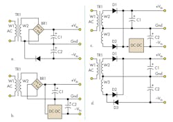
Figure 5 provides several ideas for generating the negative voltage needed to offset the ground or regulation/adjustment pins of the regulators, using the NE555 or other methods.
Petre Tzvetanov Petrov is an electronics engineer with Micro-Engineering, Sofia, Bulgaria. He has worked as a researcher and assistant professor at Technical University, Sofia, and has been an expert lecturer at OFPPT, Casablanca, in the Kingdom of Morocco. He can be reached at [email protected].
