Engineers are under constant pressure to improve the performance of their products while reducing product cost. The key to doing so is a better understanding of the power distribution network (PDN) noise path.
The minimum noise is achieved when a source, interconnect, and load are all well matched, as exemplified in many test and measurement instruments. Signal generators, oscilloscopes, spectrum analyzers, and vector network analyzers are often 50 Ω, connected using 50-Ω coaxial cables through 50-Ω connectors.
This file type includes high resolution graphics and schematics when applicable.
There are other standard impedance levels, such as the 100 Ω often used in digital pathways and 75 Ω used in CCTV. Yet all of these instruments use the matched interconnect system to maximize performance while minimizing noise. This also applies to PDNs.
Breaking It Down
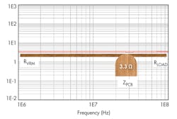
A PDN consists of a voltage regulator (VRM) and interconnecting printed-circuit board (PCB) planes, traces, and loads, which are the circuits being powered. Figure 1 illustrates the impedance of a well balanced PDN. This PDN has an arbitrary impedance of 3.3 Ω. The VRM output impedance (RVRM) is 3.3 Ω, the PCB plane impedance (ZPCB) is 3.3 Ω, and the load circuit impedance (RLOAD) is 3.3 Ω, resulting in an ideal, perfectly flat PDN as seen in the red trace.
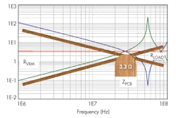
If the VRM and PDN interface becomes unbalanced in either direction, the PDN is no longer flat and is, therefore, susceptible to noise, degrading system performance. Figure 2 shows the PDN impedance for the three cases where the VRM impedance is greater than, less than, or equal to the PCB plane impedance and load impedance.
If the VRM impedance is too high, the PDN impedance looks capacitive at frequencies below the resonant frequency of the PCB planes, denoted by the 20-dB/decade decreasing impedance. If the VRM impedance is too low, the PDN impedance appears inductive at frequencies below the resonant frequency of the PCB planes, denoted by the 20-dB/decade increasing impedance.
At the load, the transmission line effects of the PCB result in a sharp peak at double the resonant frequency of the PCB plane. In the inductive case, the peak is positive, while in the capacitive case the peak is negative.
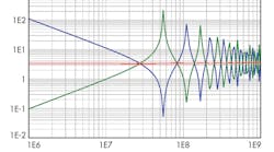
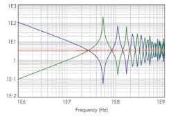
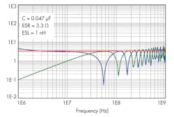
Figure 3 depicts the same three impedance traces at higher frequencies. It clearly shows the transmission line characteristics with repeating positive and negative peaks. The capacitive PCB plane results in a negative peak followed by a positive peak and repeating the pattern. In a similar way, the inductive PCB plane results in a positive peak followed by a negative peak and repeating the pattern. In either case, the positive peaks are far greater than the PCB and load impedance, and the negative peaks are far below the PCB and load impedance.
It is possible to add decoupling capacitance at the load to flatten the PDN impedance and improve the system performance. Figure 4 shows the results with a 0.047-µF ceramic capacitor added at the load.
Adding the ceramic capacitor reduced the low-frequency impedance to the level of the PCB plane impedance. The inductive peak, though reduced in frequency and amplitude, is still far greater than the PCB plane impedance. At higher frequencies, the impedance again increases above the PCB plane impedance.
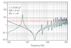
It is possible to maintain the peak impedance below the PCB impedance by using a ceramic decoupling capacitor with a series resistance (ESR) that is equal to the PCB plane impedance at all frequencies above the first resonance and a series inductance (ESL) that presents an impedance equal to the PCB impedance at the highest frequency of interest. In this case, the capacitor requires an ESR of 3.3 Ω, and the capacitor ESL must be lower than 500 pH (Fig. 5).
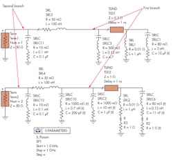
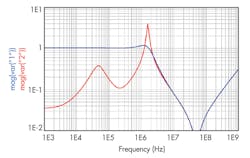
While the negative peaks are well below the PCB plane impedance, they can still degrade system performance. The impedance presented at the load is also the source to the next daisy-chained circuit. As such, this impedance needs to be equal to the plane impedance to minimize peaking at the next circuit as well (Fig. 6).
There are many ways to use these principles to reduce the cost of our designs while maintaining or improving performance:
• Consider the resistance and impedance of the VRM. A VRM that has lower impedance and better regulation is often more expensive than a higher-impedance device. If the impedance is below the characteristic impedance of the PCB, impedance peaks at the load can result.
• Don’t overdesign the PCB planes. Reducing the plane impedance requires more physical space on the PCB and can unnecessarily increase the number of layers required, increasing cost.
• Low-ESR tantalum capacitors command a higher price. A higher-ESR capacitor is often needed to maintain the PDN balance, allowing the use of lower-cost tantalum or aluminum capacitors. This is also frequently the case when paralleling bulk capacitors and decoupling capacitors. Higher-ESR bulk capacitors frequently are required to maintain the PDN balance. In some cases, it may be appropriate to add an external resistor in series with the capacitor to balance the PDN. This is often the least expensive solution to keeping the PDN balanced.
• In some cases, particularly if the regulator is a linear type of device, capacitors are not required at the regulator, only at the load.
• Be sure to assess the output impedance of all voltage regulators. This reveals the stability, a critical performance parameter. It also will show any impedance peaks that result from poor stability margins. The stability margin often can be improved by changing the value of a compensation resistor or capacitor, which is much less expensive than reducing the impedance peak using brute force filters.
• With cascaded circuits, you should make an effort to keep similar impedances together. A high-impedance circuit that follows a low-impedance circuit can result in an inductive PDN that is hard to filter, whereas similar impedances will stay in balance.
• The lowest-noise impedance occurs when the VRM impedance, PCB impedance, and load impedance are matched. This is counterintuitive, but indicates that the addition of a series resistor between the VRM and the PCB plane can reduce the voltage excursions seen at the load.
PDN Design Example
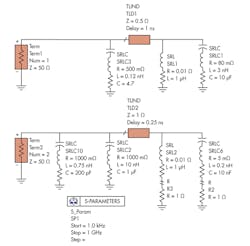
A PDN with a 2-Ω maximum impedance requirement from dc to 1 GHz uses a linear voltage regulator that can be characterized as a 1-µH inductance with a 10-mΩ series resistance. This is typical of a linear regulator operating at 100 mA and can be measured easily. Two design approaches are available (Fig. 7). One is designed with maximal flatness. The other is a typical design using low a low-ESR capacitor at the regulator and an oversized PCB plane.
Figure 8 illustrates the simulated impedance results at the load. The oversized PCB plane and low-ESR capacitor solution likely cost a bit more but result in a lower (though not flat) impedance.
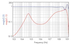
What is less obvious is that the more expensive solution may also present issues to PDN paths connected to this node, due to the low damping below 1 kHz and from 100 kHz to 10 MHz. The additional 1-Ω branch is connected to this node using a 100-nH inductor and a 100-nF capacitor (Fig. 6, again). Figure 9 shows the simulated impedance results at the second branch. Further performance improvements can be gained by adding a 1-Ω resistor in series with the 0.1-µF second-branch capacitors if the load impedance connected to this PDN node does not present a 1-Ω resistance.
By carefully matching the VRM, PCB planes, and load circuits to each other and to the required impedance magnitude, a flat PDN impedance can be created while minimizing circuit board area. The optimization also minimizes the use of expensive low-ESR capacitors and low-impedance voltage regulators.
Steve Sandler is the founder and chief engineer of AEi Systems LLC and the president of Picotest. At Picotest he is responsible for signal injector product development, as well as the overall operation of the test equipment company.
