In the world of power technology, scores of new information on the lowest, highest, smallest, densest, etc., seemingly arrives daily, leaving engineers to scramble to keep up with the latest trends. It’s those engineering teams carefully considering and selecting the latest power devices and related circuits that will likely reap the most significant performance gains. For designers starting new projects, this quick update will help in that effort—and may even influence the direction of future change.
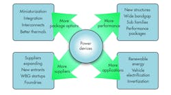
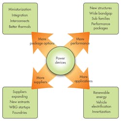
For decades, breakthroughs in technology have reshaped the power-device landscape. And the beat goes on with the latest crop of innovative device structures, thinner wafers, higher cell densities, new materials, greater integration, and new packaging technologies (see the figure).
Whether it’s higher conductivity, faster switching, more robustness, or a combination thereof, progress is evident across most product categories. Compared to a just few years ago, systems engineers working on new designs have significantly better power devices at their fingertips. This, of course, spawns multiple benefits:
This file type includes high resolution graphics and schematics when applicable.
• More performance: In addition to the aforementioned performance enablers, stratification of power-device types into many sub-families has improved performance for narrowly targeted applications. These include MOSFETs with diodes optimized for several classes of reverse recovery time (tRR), or IGBTs introduced with extended short-circuit withstand time (tSC) options.
• More packages: Taking full advantage of better devices at a system level requires new packages for smaller size, higher switching speeds, less resistance, less inductance, more integration, better thermal performance, etc.
• More applications: Power-semiconductor content continues to expand as demand grows for greater energy efficiency in applications such as handheld devices, vehicle electrification, grid storage, renewable energy, and motor-drive “inverterization.” Thus, there’s a broad trend toward higher unit volumes. On top of that, devices that feed these specific applications will likely receive more development resources while rapidly advancing up the performance ladder.
• More suppliers: Despite recent consolidations, the power-device business overall continues to add suppliers. In particular, IGBTs and wide-bandgap (WBG) devices are available from both traditional and “startup” suppliers, creating a greater array of new part, performance, integration, and packaging options. As a result, the relationship between power-device OEMs and their customers has become more important than ever.
Digging deeper on the last bullet point, power-device performance and selection is inherently tied to a load, inductor, capacitor, or heat sink that’s typically engineered on the system side. To ensure full capture of these device-level innovations at the system level, communication between power-device engineers and systems engineers is paramount. One sub-plot to it all, though, involves second-sourcing of discrete components—it’s become more difficult due to increased optimization of power devices for specific uses, meaning greater complexity when trying to match performance across suppliers.
Taken together, power semiconductors currently reside in a dynamic era of “more of everything,” particularly from the viewpoint of device users. What follows are some of the biggest movers and shakers.
25- to 30-V MOSFETs
In terms of dominance within the industry, 25- to 30-VDS MOSFETs used for dc-dc downconversion in computing applications rank right at the top. Four prominent trends highlight this arena:
• Markedly improved silicon performance: Just a few years ago, the drain-source resistance (RDS(ON)) for the top-performing syncFETs were double that of today’s equivalently packaged best devices (syncFETs were Fairchild’s original designation for FETs with integral Schottky diodes). Similar improvements have occurred with high-side FETs. Such FETs are now occasionally developed on a switching-performance-focused process that’s completely independent from the syncFET process.
• The move to 3-by-3 DFN packages and asymmetric half-bridge dual MOSFETs: These have replaced 5-by-6 dual flat no-lead (DFN) packages in many applications, much like when 5-by-6 DFNs replaced DPAKs just as a few short years ago. The move is consistent with the industry-wide trend of miniaturized integrated devices targeting applications demanding higher performance. These packaging transitions occurred within just three to four years.
• More integration for greater performance gains: To effectively reduce size, increase efficiencies, and push switching speeds to and beyond 1 MHz requires minimization of package resistance and related parasitic effect. That means greater emphasis on integration of FETs, drivers, and controllers. Integrated dc-dc converters can be partitioned in various ways. For example, asymmetric dual MOSFETs (two die in one package) come in 5-by-6, 3-by-3, or other sizes widely used in downconverters to 30 A and beyond. Or two MOSFETS plus drivers (three die in one package) can create “DrMOS” (driver-MOSFET, an Intel packaging standard) and similar multichip module devices in various packages, which handle up to 60 A at frequencies over 500 kHz. Further, two MOSFETs plus a driver and a controller (three or four die in one package) could form a point-of load (POL) device and run almost as high a current as the DrMOS type parts. Finally, monolithic components that combine the controller, driver, and high- and low-side MOSFETs in a single die can run to 15 A, with efficiencies near 90% from 100 mA to 15 A even when stepping down to 1 V from 12 V.
• Further segmentation counter trend: On the other hand, continued strong supplier support for the 25- to 30-V commodity zone may retard segmentation. For this segment, device performance significantly lags the cutting edge.
40- to 250-V MOSFETs
Key trends in this sector include:
• Many more available parts: More suppliers now develop power devices for motor drives in 48- to 80-V systems, synchronous rectification for ac-dc SMPS, isolated dc-dc converters for telecom/datacom, class-D audio amps, and UPSs.
• Much improved technology: In terms of potential performance, the new SiC and GaN semiconductor technologies developed for this segment is far superior to conventional silicon. It increased efficiency and power density, thus minimizing paralleling and board-space requirements.
• Optimized SSR devices: Solid-state-relay (SSR) devices have been optimized for RDS(ON), switching, and diode recovery losses. Low-gate charge, low-output capacitance, and reduced body-diode recovery charge helped shrink losses in non-resonant switching circuits.
400-V+ MOSFETs
The over-arching trend here revolves around high-voltage super-junction devices:
• Super-junction MOSFETs with wider voltage ranges: From a traditional base of 600 V, these devices are now available to 1200 V.
• Trench-based alternatives: Using deep-trench for charge balancing instead of multilevel-epitaxial devices—at least below 650 V—provides QG and QGD (two different definitions of gate charge) advantages that lead to reduced switching losses, with still very low RDS(ON).
• Thin SMD packaging: Low z-height surface-mount devices (SMDs), as opposed to TO-263 or TO-252, reduce size and parasitic inductances.
• Arrival of new varieties, like faster body diodes: Parts with better tRR (150 ns and lower) for hard-switched applications have become more prominent.
• Wider application of super-junction MOSFETs: These devices are now moving into consumer applications (e.g., LED lighting), ac-dc flybacks, and lower-power solar inverters for solar and battery chargers.
IGBTs
Insulated-gate bipolar transistors (IGBTs) have long maintained an amperes-per-dollar edge over MOSFETs, and that remains the case today. However, IGBTs are changing in many other ways:
• Performance boost via tradeoffs: Major recent improvements, and those on the horizon, have and will be realized thanks to the three-way tradeoff among conduction performance (as measured by VCE(SAT)), switching performance (as measured by tF), and ruggedness (as measured by tSC). For example, 100-A IGBTs with 10-μs tSC are now available with typical VCE(SAT) = 1.5 V @ 50 A and TF = 80 ns. Just a few years ago, such a performance level would have required a device with a much lower tSC.
• Availability of higher-current IGBT die: Such die, rated to hundreds of amperes, can help lessen the need for paralleling IGBTs, which brings added design challenges.
• Better monolithic reverse-conducting IGBT performance: The spike in performance makes it possible to reach more applications like resonant converters and small motor drives.
• Continued dominance of modules: One speculated trend, for reasons of cost and design flexibility, was a gradual migration from module- to more discrete-based designs. It hasn’t happened, though. However, the integration advantages of modules for performance, size, and design simplicity remain powerful traits. Hybrid modules with an IGBT matched to a silicon-carbide (SiC) diode have emerged to further address IGBT limitations. Even full SiC-based solutions can be found.
• IGBTs and MOSFETs remain app-specific: Despite significant performance improvements from both IGBTs (faster) and MOSFETs (lower RDS(ON)), there’s been little sign of traditional MOSFET applications moving to IGBTs or vice versa.
WBG Devices
Wide-bandgap trends show that the devices are making inroads, though it’s been slow:
• Dominant footing in some spots: A common perception is that costs must decrease before there’s any widespread adoption of WBG devices. However, when conditions are right, such as in the power-factor-correction (PFC) diode socket of high-end power supplies, WBG-device performance outweighs its higher cost when trying to meet stringent efficiency standards.
• WBG switch adoption remains low: To justify the use of higher-cost WBG devices, a system overhaul, including shrinking heat sinks, inductors, and capacitors, is needed to reduce cost and boost performance. This is even evident for applications such as renewable energy (or electric vehicles)—straight device performance directly translates into better end-product performance, yet WBG can’t seem to make a dent.
• Cost reductions will ultimately accelerate adoption: It’s a synergistic loop—greater adoption will drive down costs, which will drive greater adoption. Early inroads, such as 1200-V SiC MOSFETs into formerly pure IGBT territory (e.g., high-power solar inverters), will catalyze this loop.
Packaging Trends
Breakthroughs at the silicon level (or GaN or SiC) often necessitate better packages to take full advantage of the possible performance, as well as skirt the parasitic inductance and resistance limitations of traditional packages. Examples include leadless or minimal-lead SMD packages to replace TO-263s and TO-252s, the use of chip-scale packages for low z-height requirements, and embedded packaging to maximize thermal performance. Another example is the hole-less TO-247 package. These packages enable larger devices and offer increased power output compared to standard TO-247s.
Another growing trend is the deployment of wire-bonding alternatives. Straps and clips can often replace wire bonding to maximize performance. Clips even enable higher currents in new packages, allowing migration away from through-hole packages such as TO-247s. Also trending is a rapid increase in integration. Development of new modules and multi-chip packages has sharply risen across all power levels, particularly for very-low and very-high voltages.
Power devices are no longer just a mix of a few TO-247 and TO-263 devices. A complex interaction of device R&D and packaging advances, plus a growing application, customer, and supplier base, have quickened the pace of power-device evolution. Designers can adopt simple practices to take advantage of these developments:
• Check datasheet revision dates on power-device choices. If the part is more than three or four years old, significantly improved devices are probably available.
• Look beyond previously preferred suppliers for better alternative devices.
• Check for new package options. If better versions are available, but lack the right device rating, suppliers may offer the preferred silicon in the new package upon request.
• If the power devices are critical to performance, maintain a close relationship with suppliers for customized solutions.
• Change products, such as IGBTs instead of MOSFETs, or WBG instead of either, to create new opportunity.


