Thoughtful Board Design Unlocks the Promise of GaN
Download this article in .PDF format
Power transistors with faster switching speeds will enable power supplies with smaller form factors and higher energy transfer efficiencies. Indeed, the elimination of heat sinks will give designers the ability to visualize entirely new form factors for power bricks and modules, including those enabling wireless power transfers. Companies like Texas Instruments and Efficient Power Conversion (EPC) are focusing on applications requiring compact form factors and high energy-transfer efficiencies.
Incorporation of gallium-nitride (GaN) transistors, fabricated on inexpensive silicon substrates, represents an improvement over conventional silicon MOSFETs. The faster switching speed and lower on-resistance of GaN devices makes possible smaller devices with lower heat dissipation. Low-voltage transistors in chip-scale packaging have footprints as small as 0.9 × 0.9 mm. Thus, with thoughtful board and package design, low-voltage GaN devices can shrink the size of power bricks and modules.
However, the substitution of GaN transistors for MOSFETs is not one-to-one. The layout must minimize the inductive path between the power-stage devices and their drivers to avoid impairing performance. And gate-drive requirements will vary from one GaN device to another; low-voltage devices can be sensitive to overdrive.
Board layouts for GaN transistors must account for parasitics, which are less prominent in slower MOSFET systems. Particularly, designers must minimize the inductive path between the source of the driver and the FET transistor’s gate. Without that, says TI’s Systems Architect Michael Seeman, it’s like installing a 500-hp engine under the hood of an economy car. Without a matching frame transmission, and suspension, you can do serious damage.
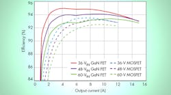
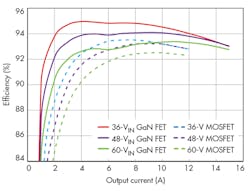
1. The graph displays GaN FET efficiency versus a traditional MOSFET.
As a result, engineers using GaN must isolate the source-to-gate-drive path from any common-mode inductances. (EPC’s transistors fortunately use a low-inductance package with solder bar interconnects.) The avoidance of overdrive is another serious engineering issue: EPC’s eGaN FETs can be damaged by gate drive greater than 6 V. Consequently, some FET drivers (like TI’s LM5113) will hold the GaN FET drive to 5.25 V with an internal clamping circuit.
Improved POL Efficiency: Low-Hanging Fruit
The existing literature (pairing the LM5113 gate driver, for example, with EPC2001 eGaN FETs) compares the design of a dc-dc power converter using 36-V GaN transistors to a dc-dc with 36-V silicon MOSFETs. By eliminating heat sinks, the brick using GaN FETs is a fraction of the size of the brick using FETs. And a small but significant difference occurs in energy transfer efficiency.
Not surprisingly, the dc-dc with 36-V GaN FETs showed the highest efficiencies, better than 94% for current loads from 2A to 12A (better than 92% out to 15 A) (see “Gate Drivers for Enhancement Mode GaN Power FETs”). Among the 60-V circuits, the GaN FETs offered better than 92% for all loads above 4A, while the MOSFET efficiency reached 92% only above 6A (Fig. 1).In a 1/8th brick converter dropping a 36- to 75-V input to a fixed 12-V output, the operation of several low-voltage GaN FETs was compared with MOSFETs with the same voltage and current ratings. The efficiency of a 36-V GaN FET was compared with the efficiency of a 36-V MOSFET; the efficiency of a 48-V GaN FET was compared with a 48-V MOSFET, and so on for 60-V systems. Switching speeds for higher-voltage devices under load are a bit slower than lower-voltage devices. But in this demonstration, the devices were clocked similarly: The dc-dc converter with GaN FETs was clocked at 333 kHz, while the circuit with MOSFETs was clocked at a familiar 250 kHz.
In a similar demonstration, the efficiency of a 48- to 12-V switching regulator using TI’s LMG5200 driver circuit pushing 80-V GaN FETs was compared with a MOSFET-based dc-dc converter (see “GaN FET Module Performance Advantage over Silicon”). The LMG5200 incorporates a controller/driver and two 80-V FETs in a 6- × 8-mm QFN package. In the efficiency demonstration, it was clocked at 1 MHz.
The MOSFET-based implementations were switched at a conventional 250 kHz and again at 800 kHz. Predictably, the circuit with GaN transistors exhibited fewer switching losses. The 80-V MOSFET at 250 kHz actually delivered better than 92% efficiency under a range of current loads out to 6 A. The LMG5200 circuit demonstrated better than 94% efficiency from 4 to 10 A.
In point-of-load (POL) supplies, the difference in efficiencies—even 1% or 2%—can be significant. In a telecomm switching station, for example, where a 48-V intermediate voltage must be dropped to 12 V or less on literally thousands of POL supplies, the savings in electrical energy can amount to thousands of dollars per year. For dc-dc converters, consequently, GaN is an enabling technology.
The Anatomy of a Switching Regulator
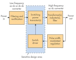
In operation, a dc-dc converter is essentially a power pump, based on a sawtooth oscillator, drumming out pulses at a predictable cadence. (The voltage and currents applied to the load are governed by the width and frequency of the pulses.) Three essential elements make up the chain (Fig. 2):
• A pulse-width modulator (PWM), and control logic.
• A power stage (typically two power transistors, a high-side and low-side device, and their gate drivers), which pulls current from the power source, and feeds it to the load.
• An LC network to smooth the pulses.
2. Generic functions of a switched-mode power supply include a pulse-width modulator, power stage, and LC network.
The operation of a switching power supply (overly simplified) can be visualized as a steam shovel moving a mountain of dirt from one location to another. Think how long it takes the shovel to scoop up the dirt in one place and dump it at another. Think how much dirt is left behind. Imagine what the transfer would look like if the steam shovel were replaced by a teaspoon making dirt transfers a million times a second. This is a model for a switching power supply of the future—ever faster and smaller energy transfers.
But switching power pulses under load remains a challenge: The higher the voltages and currents moved, the more sluggish the switching speeds are likely to be. Thus, the sweet spot for switching power-supply design remains doggedly at 250 kHz. There are high-efficiency parts operating at 1-MHz commutation rates, but switching regulators operating at (say) 10 MHz (and small enough to incorporate spiral inductors on-chip) are still a rarity.
GaN’s faster switching speeds, despite the attention required for packaging and board layout, are an enabler for power-supply efficiencies. At the very least, it reduces the size and cost of the inductors. Longer term, it allows for a re-invention of the power-management function. GaN devices are considered high electron mobility transistors (HEMTs). The availability of “enhancement-mode devices,” which enable GaN transistors to turn-on/turn-off with the application of positive gate voltages, will encourage MOSFET system builders to experiment.
The TI LMG5200 GaN FET power stage EVM actually serves as an evaluation tool for potential GaN converts. TI says the LMG5200, by itself, offers measurable performance improvements across a wide variety of applications. These applications include multi-megahertz synchronous buck converters, Class D amplifiers for audio, and 48-V POL converters for telecommunications servers.


