This file type includes high-resolution graphics and schematics when applicable.
Efficiency is one of the key goals in power-supply design. Meeting this objective not only saves energy, but also reduces heat. Traditional analog power supplies don’t meet these objectives, so most new designs today are switch-mode power supplies (SMPSs). SMPSs use a mix of high-frequency switching, energy storage, and filtering to achieve efficiencies of 70% to over 90%, depending on the configuration and application. Some examples include dc-dc converters, regulators, inverters, and battery chargers.
One way to improve efficiency is to use high voltages and minimize the number of power-conversion stages used in the supply. High voltage always produces greater efficiencies in power delivery and conversion. For instance, power utilities have known for a generation or more that stepping up the ac voltage before long-distance transmission produces considerably less loss in the lines. Voltages are stepped up to tens of thousands or hundreds of thousands of volts before transmission.High Voltage Leads to Greater Efficiency
The same concept applies in SMPS design. Keep the voltage high for as much of the process as possible and reduce the number of stages that produce power conversion. Each stage decreases the overall efficiency. The goal is to bring high input voltage into or as close to the end equipment output as possible before downconversion. Fewer power conversions mean greater efficiency.
Isolation
When high voltage is used along with traditional lower voltages, some form of isolation is needed to protect the lower voltage circuitry. One solution is to use transformers. Heavily insulated windings and magnetic coupling ensure excellent partitioning of circuitry. However, a transformer adds unwelcome extra cost, space, and weight to the design. Another alternative is to incorporate an optocoupler, although it may not be fast enough for the design. The best option, then, is to use capacitive isolation. ICs with such isolation are now available.
High-voltage SMPSs can greatly improve special industrial power devices. Some examples include half-bridge and full-bridge converters, solar inverters, motor drives, UPS and special supplies for data-center server farms, telecom, and industrial infrastructure. What’s required to achieve the desired efficiency is a mix of high-voltage power devices as well as special ICs to drive them.
Most SMPSs implement a closed-loop design, where feedback in the form of pulse-width modulation (PWM) is use to control pulse duty cycle and output-voltage level. The PWM signals come from low-voltage ICs whose output levels are way too small to control the output-power devices like MOSFETs or IGBTs. What’s needed is some form of gate-drive circuitry that conditions the low-level PWM signals to appropriate drive levels while providing some isolation protection from the high voltages. There are two basic drive methods: gate-drive transformers and high-voltage high-side/low-side IC drivers.
Gate-Drive Transformers
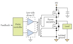
Traditionally, a transformer delivers the gate-drive signals to power MOSFETs or IGBTs. Figure 1 shows a simplified arrangement. The transformer takes care of most of the driver needs. The windings’ turns ratio provides the correct drive levels and, at the same time, isolation is assured thanks to the insulated windings and magnetic induction.
The downsides to the transformer solution are dc core saturation (unless there’s capacitive coupling on the primary), inter-winding capacitances that create parasitic effects, and effects produced by leakage inductance. Additional components are often needed to protect the output devices. More important is the disadvantage of transformer size, volume, weight, and cost.
High-Side/Low-Side Driver
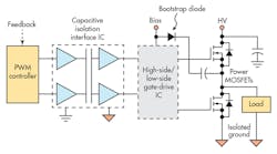
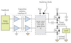
A simplified high-side/low-side driver solution is illustrated in Figure 2. The high-side/low-side driver is a special IC designed to produce the necessary gate-drive signals to the output devices. Such an IC has two channels, one for each output device—one channel is ground-referenced and the other is floating. It’s important to note that it requires a bootstrap bias supply. Also, isolation is usually provided by a digital isolator IC that uses capacitive-coupling stages for the isolation barrier.
The benefit of the high-side/low-side driver is that it wipes out all of the transformer disadvantages: Volume and PCB space savings are significant, and it cuts down on overall component count. The only requirement is an extra bias supply.


